Reference technology and specs
Reference technology and specs
In this segment of the article we will look at the reference (original design) based specs and architecture. The GeForce GTX 650 is based on the Kepler GPU architecture. The product however is using a new chip called the GK107 which is based on a 28nm fabrication process. The chip has a transistor count of 2.54 Billion for those that care.
When we peek at NVIDIA's slide decks we see them denoting that the GeForce GTX 650 has been designed for 1080p gaming with medium settings and FXAA. That's true but please do understand this remains a budget level graphics card .
- The GeForce GTX 650 boasts 384 CUDA (shader) cores
- The GeForce GTX 660 boasts 960 CUDA (shader) cores
- The GeForce GTX 660 Ti boasts 1344 CUDA (shader) cores
- The GeForce GTX 670 boasts 1344 CUDA (shader) cores
- The GeForce GTX 680 boasts 1536 CUDA (shader) cores
The GeForce GTX 650 ships with 2 SMX units containing 384 CUDA Cores and 32 texture units. The graphics core clock speed of the GeForce GTX 650 is 1058MHz. GPU Boost is not available. The GeForce GTX 650s memory speed is 5000MHz data rate.
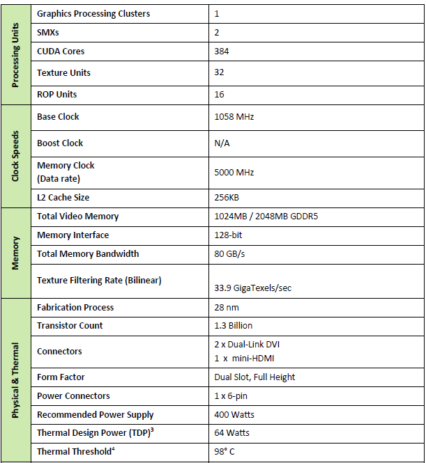
With a TDP of just 64 watts, the GeForce GTX 650 draws very little power though, it still ships with an external power connector. This power connector provides additional headroom for overclocking. Many GeForce GTX 650 boards are capable of hitting speeds in excess of 1200MHz.
The idle power of GeForce GTX 650 is ~5W representing best in class idle power. In addition, HD video playable is ~13W, again representing best in class power consumption.
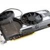
The GeForce GTX 650 reference board measures 5.7 in length. Display outputs include two dual-link DVIs and one mini-HDMI. One 6-pin PCIe power connector is required for operation.
128-bit Memory Interface
The memory subsystem of the GeForce GTX 660 consists of two 64-bit memory controllers (128-bit) with either 1GB or 2GB of GDDR5 memory.
We already mentioned it, another change is the ROP (raster operation) engine, cut down to 16 units opposed to 24 on it's bigger brother the GTX 660. With this release, NVIDIA now has the real mid-range products on its way. The new graphics adapters are of course DirectX 11.1 ready.
With Windows 8, 7 and Vista also being DX11 ready all we need are more new games to take advantage of DirectCompute, multi-threading, hardware tessellation and the latest shader 5.0 extensions. For your reference here's a quick overview of some of the more recent graphics cards.
| GeForce GTX 650 |
GeForce GTX 660 |
GeForce GTX 660 Ti |
GeForce GTX 670 |
GeForce GTX 680 |
GeForce GTX 690 | |
| Stream (Shader) Processors | 384 | 960 | 1344 | 1344 | 1536 | 3072 |
| Core Clock (MHz) | 1058 | 980 | 915 | 915 | 1006 | 915 |
| Shader Clock (MHz) | 1058 | - | - | - | - | - |
| Boost clock (Mhz) | - | 1033 | 980 | 980 | 1058 | 1019 |
| Memory Clock (effective MHz) | 5000 | 6008 | 6008 | 6008 | 6008 | 6008 |
| Memory amount | <2048 | 2048 | 2048 | 2048 | 2048 | 4096 |
| Memory Interface | 128-bit | 192-bit | 192-bit | 256-bit | 256-bit | 256-bit |
| Memory Type | GDDR5 | GDDR5 | GDDR5 | GDDR5 | GDDR5 | GDDR5 |
For Kepler, NVIDIA kept their memory controllers GDDR5 compatible. Memory wise NVIDIA has nice large memory volumes due to their architecture, we pass 2 GB as standard these days for most of NVIDIA's series 600 graphics cards in the high range spectrum. We expect most GTX 650 cards to come with 1 GB of graphics memory in order to remain price competitive.
