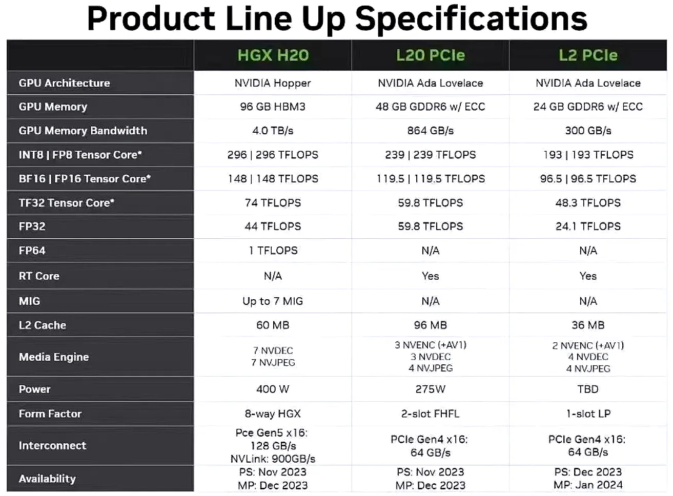
The upcoming HGX H20 is engineered with 96GB of HBM3 memory and offers a memory bandwidth of 4.0 terabytes per second (TB/s), which represents an increase from the H100's 3.6 TB/s. It is built on the Hopper architecture, which enhances its computing performance. The NVLink bandwidth within this architecture is upgraded to 900GB/s, in comparison to the 400GB/s of the A800, reflecting the advancements to accommodate increased bandwidth demands.
The L20 PCIe is another addition, utilizing the AD102 chip and equipped with 48GB of GDDR6 memory with Error-Correcting Code (ECC). NVIDIA has made adjustments to this model to align with the 4800 Total Performance Processing (TPP) threshold, resulting in a Total Graphics Power (TGP) of 275 watts, which is lower than the GeForce RTX 4090's 450 watts. The L2 PCIe, sharing the Ada Lovelace architecture with the L20 PCIe, is anticipated to use the AD104 chip, judging by its specifications.
While the verification of these details is pending, the information, presumably released by NVIDIA, holds a high degree of plausibility. The introduction of the HGX H20, L20 PCIe, and L2 PCIe demonstrates NVIDIA's commitment to innovating within the regulatory boundaries and continuing to support the Chinese market's needs.