Technology and Photo's
Right, overclockerz .. As you can notice this product is made for exactly this category. People who tweak the most out of their system. To be able to test this product to it's fullest potential we will need to overclock the PC, and of course we'll do just that. We'll check this product with aggressive BIOS ram timings and CAS 2 (Column Address Strobe) latency to see where it halts. In this test we will make use of a test system that allows overclocking and memory tweaking from within the BIOS. The mainboard can handle a DDR:CPU ratio of 2x, 2.5x and 3x. We'll test the sample at both normal and aggressive ram timings.
Oh and for your information, the EL in EL DDR is not named after some kind of Mexican food or something, EL simply means Enhanced Latency.
The ModuleLet's take a closer look at the module.
The module is constructed out of a six layer PCB and equipped with 4.5ns memory. This module in fact supports a CAS latency of 2 at 2.5v (default).
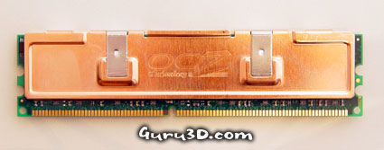
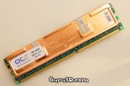
You have to admit, the copper heat spreader is looking fancy. In fact it's one of the most beautiful looking modules I have seen. Of course it's on there to remove and dissolve heat as fast as possible from the memory chips. The choice for copper is a good one as it absorbs heat extremely well. The heat spreader is firmly attached to the module. No colored PCB and furthermore the module looks very well-built, the performance test we ran can prove just that.
| Test system |
|
* disabled while benchmarking |
I have to make an additional side-note on our test-method. It was very hard to test this memory module at it's maximum potential, this is not because of the El DDR PC3500 memory module but because of our test system. Let me explain, this test rig we used makes use of a Intel engineering sample Pentium 4 2.4 GHz processor and Intel PX845PE mainboard. Under the ideal circumstances we would have lowered the tact frequency of the processor and then increase the Front Side Bus speed of the Pentium 4. That way we would have been able to test the memory way beyond specifications. Unfortionately our mainboard does not allow changing the Clock Frequency of our unlocked Pentium 4 Processor (18x). Therefore we can only pump up that FSB until the CPU can't go any further. We got it at (4x)155MHz which is not a bad results at all yet not quite enough to max out this memory. As result we where only able to test the Memory module at 414 MHz while it should be able to handle 433 MHz straight out of the box. On the other hand .. it's close enough if we trhow some agrresive RAM timings at it.
