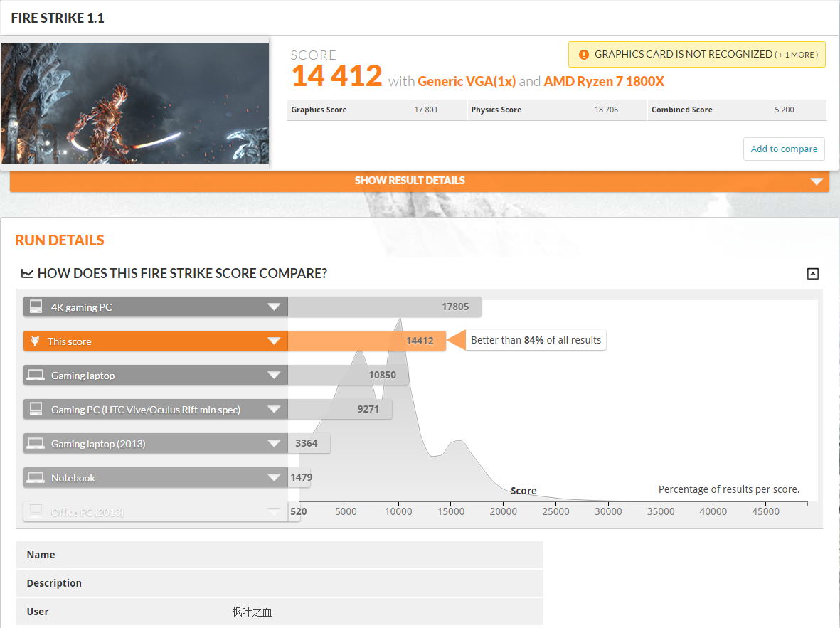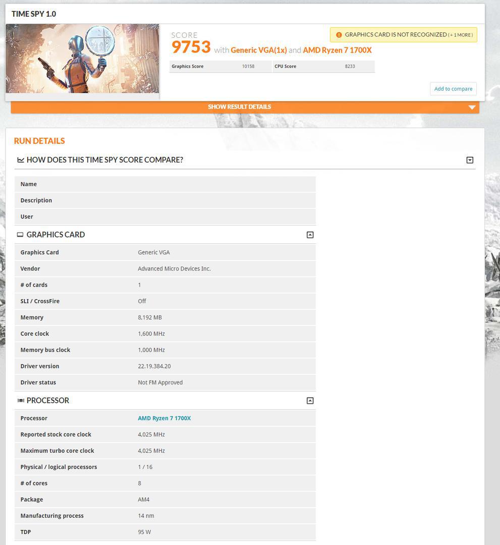
Last week a 3Dmark Time Spy result set and Vega details have already seen and detected by one of our forum member, this weeks startes with a FireStike P score result set. Again with a Vega at a 1200 MHz GPU clock and 700 MHz HBM2 VRAM clock.
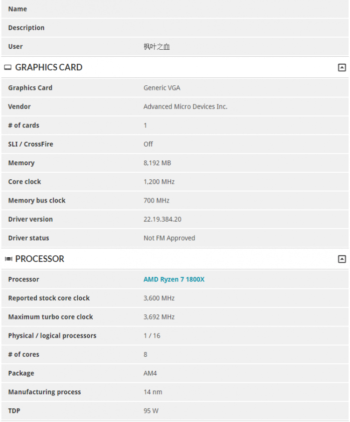
The Radeon RX Vega card tested was tagged with ID 687F:C1 and shows a graphics score of 17801. Specs for Vega include 64 CUs x 64 shader units = 4096 shader processors. These are divided over four blocks. There is a total of 64 ROP units (16 per block) and the GPu is to get 256 Texture memory units. If you compare it, that pretty much twice a Radeon RX 570. The architecture details actually also show a lot of similarities with Fiji (Radeon R9 Fury (X)). Vega 10 in its simplest model is expected to battle the GeForce GTX 1070 and 1080.
As it turns out, AMD could be fabbing three models:
- BIG WC = 687F:C3
- BIG Air = 687F:C2
- 'Normal' VEGA = 687F:C1
The result set from the run below this is the 687F:C1 one. The specs listed in the 3DMark scores show a device ID that is similar to that of the earlier Vega 10 prototypes we have spotted. This unit has 8GB of video RAM running at 700MHz (HBM2) and the card’s GPU clock is a 'safe' 1200MHz. So from the looks of it, these might be results from that early engineering sample. I do expect that AMD would be able to reach a 1.5 GHz base clock on the final products. Below the new entry, I also added the Time Spy one.
New Vega 10 687F:C1 3DMark Fire Strike Performance Result Spotted