Specifications
Specifications
So today NVIDIA will add one new graphics card to their line-up of two already existing high-end class DirectX 11 products. The chip used is still the GF100, not the GF104 as some of you assumed (that likely will become the GTX 460), but here's an overview of NVIDIA's DX11 class graphics card line up as of today.
- GeForce GTX 480 : 480 SP, 384-bit, 250W TDP, US$ 449~499
- GeForce GTX 470 : 448 SP, 320-bit, 225W TDP, US$ 299~349
- GeForce GTX 465 : 352 SP, 256-bit, 200W TDP, US$ 279~289
The GeForce GTX 400 is all about it's shader processors. The Fermi architecture, the GF100 graphics processor has sixteen shader clusters embedded in it (called SM short for Streaming Multiprocessor). For the GeForce GTX 480 one such a cluster is disabled, and on the GeForce GTX 470 two are disabled. For the GeForce GTX 465 we see a total of 11 active SM clusters, meaning a total of 5 are disabled inside that GF100 GPU. The core frequency of the GPU (ROPs domain) will be clocked at 607 MHz, this is tied to the shader processor domain in a 2:1 ratio, thus the Shader processors will have a 1215 MHz clock frequency.
The GF100 GPU is then placed onto an 8-layer PCB and paired with gDDR5 memory. NVIDIA made their memory controller GDDR5 compatible, which was not the case on GT200 based GeForce GTX 260/275/285/295, hence their GDDR3 memory. The GTX 465 will carry a framebuffer of 1024MB.
- The GTX 465 has four memory controllers (4x256MB) = 1024 MB of GDDR5 memory
- The GTX 470 has five memory controllers (5x256MB) = 1280 MB of GDDR5 memory
- The GTX 480 has six memory controllers (6x256MB) = 1536 MB of GDDR5 memory
As you can understand, the memory partitions, bus-width and combination of GDDR5 memory (quad data rate) allows the GPU to work with a very high framebuffer bandwidth. So we had a chat about the GF100 GPU and memory.
| GeForce 9800 GTX |
GeForce GTX 285 |
GeForce GTX 465 |
GeForce GTX 470 |
GeForce GTX 480 | |
| Stream (Shader) Processors | 128 | 240 | 352 | 448 | 480 |
| Core Clock (MHz) | 675 | 648 | 607 | 607 | 700 |
| Shader Clock (MHz) | 1675 | 1476 | 1215 | 1215 | 1400 |
| Memory Clock (datarate MHz) | 2200 | 2400 | 3206 | 3350 | 3700 |
| Memory amount | 512 MB | 1024 MB | 1024 MB | 1280 | 1536 |
| Memory Interface | 256-bit | 512-bit | 256-bit x2 | 320-bit | 384-bit |
| Memory Type | gDDR2 | gDDR3 | gDDR5 | gDDR5 | gDDR5 |
So the GeForce GTX 465 has a good amount of memory alright, 1024MB of GDDR5 memory which is tied to a 256-bit memory bus that binds to four memory controllers inside the GPU; four memory controllers x 64-bit = 256-bit. This memory is clocked at 800 MHz (= 3200 MHz effective (quad data rate memory)).
Let's take it to the next step now and look at more in-depth specifications.

So we talked about the core clocks, specifications and memory partitions. Obviously there's a lot more to talk through. Again, for an in-depth explanation of the GF100 architecture please visit this article we wrote earlier this year.
Now, at the end of the pipeline we run into an improved ROP (Raster Operation) engine, the GeForce GTX 480 has 48 units, the 470 has 40 and the GTX 465 has 32 for features like pixel blending and AA. And then for texture units the math is simple here, each SM has four texture units tied to it.
- GeForce GTX 465 has 11 SMs X 4 Texture unit clusters = 44 units
- GeForce GTX 470 has 14 SMs X 4 Texture units clusters = 56 units
- GeForce GTX 480 has 15 SMs X 4 Texture units clusters = 60 units
- A fictional GeForce GTX 485 would have 16 SMs x4 TUs = 64 units
What's also interesting about the GTX 400 release, but was a challenge, is the move towards a smaller die and fabrication process (40nm) which often brings several advantages. One advantage is that you can insert more transistors into the silicon; as such the GF100 GPU comes with 3 billion transistors embedded into this GPU (partly un-used on the GTX 465).
The GeForce GTX 465 comes with two 6-pin PEG connectors each delivering 75W and another 75W over the PCIe slot = 225W. The card targets a price point around 279 EUR / USD.
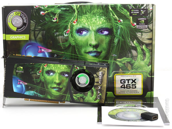
The boards tested today come from Point of View. These cards are in fact reference boards, thus the clocks frequencies and configurations are all the same.