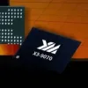
Yangtze Memory Technology Corporation (YMTC) is progressing in the development of its 3D NAND memory technology, specifically its Xtacking 4.0 architecture. This initiative has resulted in the introduction of two primary devices: a 128-layer three-bit-per-cell (TLC) 3D NAND, designated as X4-9060, and a 232-layer TLC 3D NAND, known as X4-9070.
YMTC is not currently seeking to increase the layer count beyond these models, although further expansion within the Xtacking 4.0 series is under consideration. The architecture employs a string stacking methodology, which facilitates the construction of NAND arrays with effective active layers of 64 and 116. This design strategy enables YMTC to navigate export regulations of the United States, contingent on acquiring the necessary export license from the U.S. Department of Commerce.
The specific benefits of the Xtacking 4.0 technology are not fully disclosed, but YMTC's previous developments have consistently delivered enhancements in data transfer speeds and storage density. The Xtacking 4.0 architecture is anticipated to continue this trend, potentially through the augmentation of plane counts to improve parallel processing capabilities, the refinement of bitline and wordline configurations to decrease latency, and the adjustment of chip variants to advance production yields.
For over a year, YMTC has been producing the Xtacking 3.0 version of its 232-layer TLC NAND memory and has expanded its portfolio to include both 128-layer TLC and 232-layer four-bit-per-cell (QLC) variations. These products are aligned with the current U.S. export controls pertaining to Chinese companies. Xtacking 3.0 technology incorporates string stacking and hybrid bonding techniques while utilizing a more mature process node for the chip's CMOS underlayer.
According to regulations from the U.S., the Netherlands, and Japan, manufacturers of equipment for creating 3D NAND structures with 128 layers or more must obtain export licenses. Conversely, wafer stacking with sub-128 layers does not appear to be subject to such stringent restrictions, which may allow for the continued sale of certain manufacturing tools to Chinese firms. String stacking diverges from traditional wafer bonding practices by stacking 3D NAND structures atop one another within a single wafer. This method presents an alternative compliance strategy with respect to the outlined regulations.

