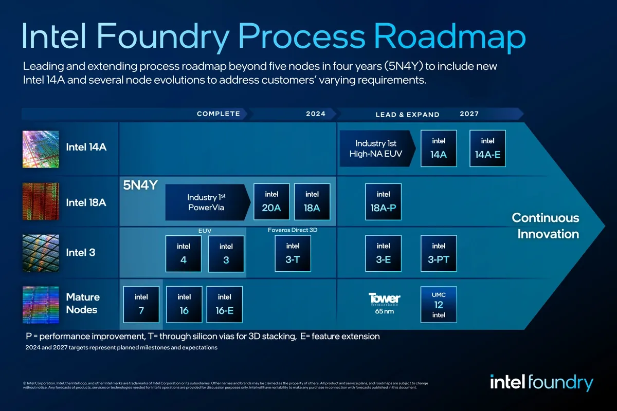
Intel has already received the initial modules of ASML's high-NA test equipment, preparing for the commencement of mass production using this technology by 2025, aligning with ASML's projected schedule. Intel has yet to release specific performance and transistor density metrics for the 14A nodes, and the schedule for production start is not confirmed. However, test production for the 14A-E version is targeted for 2027. The company's roadmap also introduces further process variations, marked with suffixes like 'E' for expanded features, 'T' for through-silicon via optimization, and 'P' for performance improvements, mirroring the approach of other industry leaders like TSMC and Samsung to cater to diverse application needs.
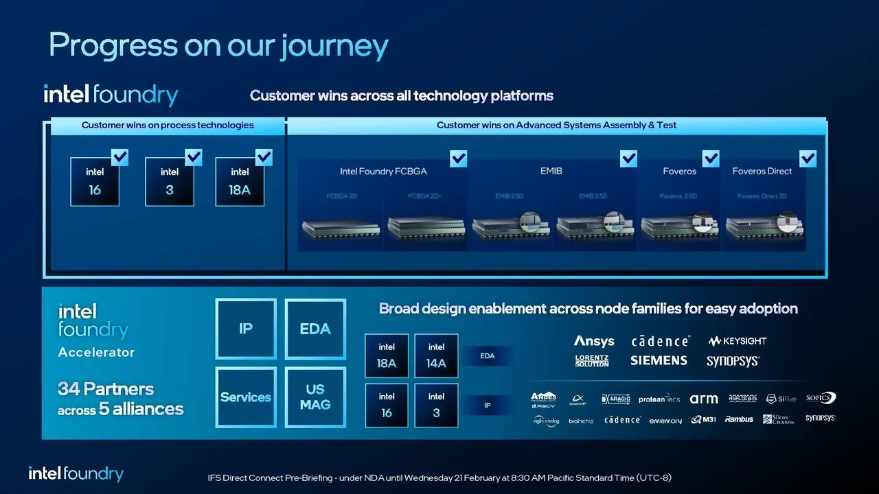
Intel is pursuing several development initiatives, including the Intel 3 series and a collaboration with UMC on the 12nm node. Renamed from Intel Foundry Services, Intel Foundry is broadening its clientele, undertaking major projects such as manufacturing chips for Microsoft using the 18A process.
This roadmap update underscores Intel's strategic direction in the semiconductor sector, highlighting its focus on advanced manufacturing capabilities and partnership expansion.