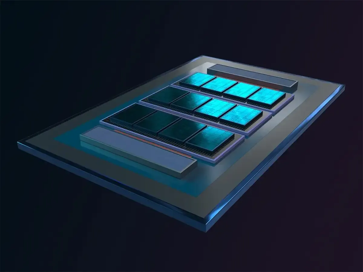
The processor's architecture encompasses up to 12 computing chiplets fabricated using Intel's 18A process technology. These chiplets prioritize energy efficiency and are central to the processor's computing capabilities. Additionally, the architecture includes up to three basic chiplets constructed with Intel's 3 process technology. These chiplets house the main cache, voltage regulation circuits, and an internal network, essential for the processor's operation. The design also features up to two I/O chiplets, manufactured using the Intel 7 process, similar to those in the Sierra Forest and Granite Rapids processors. This multi-chiplet approach allows for a modular design, facilitating the integration of components optimized for their specific functions.
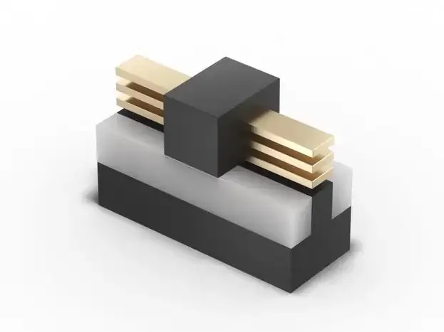
Intel's use of Foveros Direct 3D technology enables high-density interconnections between the computing and basic chiplets, ensuring efficient data transfer within the processor. Despite advancements in semiconductor technology, Intel's data center technology director, Eric Fetzer, noted that non-logic components, such as SRAM cache and high-speed I/O, derive marginal benefits from process scaling. This insight led to the strategic separation of these components from the logic chiplets in the Clearwater Forest design, addressing yield challenges associated with large monolithic chips.
Fetzer also highlighted the energy efficiency of the Foveros Direct 3D interconnects, with cross-chip data transmission energy consumption matching that of intra-chip transfers. Furthermore, the transition to RibbonFET transistors in the 18A process is expected to offer enhanced performance flexibility compared to traditional FinFET technology. RibbonFET's design allows for continuous adjustment of transistor width, providing a more dynamic approach to scaling current and improving performance.
Source: ithouse
