
Maxwell Graphics Architecture
Technology & Specifications (Reference)
The GeForce GTX 970 and 980 are based on the latest iteration of Maxwell GPU architecture, the cards use revision A1 of GM204, as explained the 20 nm node is not yet ready and these products are based on a 28 nm fab node. That will make the chips relatively large in size. Maxwell is an advanced design, it has 5.2 Billion transistors tucked away in a S-FCBGA chip. It has a 398 mm² die size. GeForce GTX 970 comes with 1664 CUDA (shader) cores while its bigger brother the GeForce GTX 980 has 2048 shader processors. The change in shader amount is among the biggest differentials together with ROP (64!) and TMU count.
- GeForce GTX 970 has 1664 shader processors and 4 GB of gDDR5 graphics memory (3.5 GB effective at full speed).
- GeForce GTX 980 has 2048 shader processors and 4 GB of gDDR5 graphics memory.
The product is obviously PCI-Express 3.0 ready, it has a max TDP of around 165 Watts with a typical idle power draw of 10 Watts. That TDP is a maximum overall, and on average your GPU will not consume that amount of power. But let me show you the coolest photo of the GPU die:
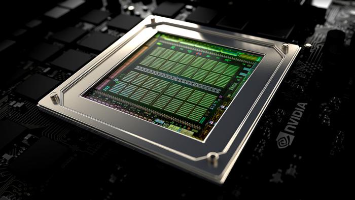
NVIDIA GM204 Maxwell architecture GPU - you can see the SMX clusters.
The GM204 is based off the Maxwell architecture, as such you will get the pre-modelled SMX clusters of what is now 128 shader processors per cluster (used to be 192 on Kepler). There are 16 active clusters for the GTX 980, times 128 shader processors which thus offers you 2048 shader processors. The reference GeForce GTX 980 has a core clock frequency of 1126 MHz with a Boost frequency that can run up to 1216 MHz.
The GTX 970 on the other hand has 13 of these clusters available x 128 = 1664 shader processors, there the base clock freqeuncy is 1050 MHz with a boost frequency up-to 1178 MHz.
As far as the memory specs of the GM204 Maxwell GPU are concerned, these boards will feature a 256-bit memory bus connected to 4 GB of GDDR5 video buffer memory, AKA VRAM AKA your framebuffer AKA graphics memory for the graphics card. On the memory controller side of things you'll see that the reference memory clock (effective data-rate) is now set at 7 GHz / Gbps.
For your reference here's a quick overview of some past generation high-end GeForce cards. Yes, the Maxwell products might seem slower if you look at the specs, but they are heavily optimized and are running at fairly high clock frequencies.
| GeForce GTX | 780 | Titan | 780 Ti | Titan Black | Titan Z | 970 | 980 |
| Stream (Shader) Processors | 2304 | 2688 | 2880 | 2880 | 5760 | 1664 | 2048 |
| Core Clock (MHz) | 863 | 836 | 875 | 889 | 705 | 1050 | 1126 |
| Boost Clock | 900 | 876 | 928 | 980 | 876 | 1178 | 1216 |
| Memory Clock (effective MHz) | 6000 | 6000 | 7000 | 7000 | 7000 | 7000 | 7000 |
| Memory amount | 3072 | 6144 | 3072 | 6144 | 12288 | 4096 | 4096 |
| Memory Interface | 384-bit | 384-bit | 384-bit | 384-bit | 384-bit | 256-bit | 256-bit |
| Memory Type | gDDR5 | gDDR5 | gDDR5 | gDDR5 | gDDR5 | gDDR5 | gDDR5 |
| HDCP | Yes | Yes | Yes | Yes | Yes | Yes | Yes |
| Display Port | Yes | Yes | Yes | Yes | Yes | Yes | Yes |
| HDMI | Yes | Yes | Yes | Yes | Yes | Yes | Yes |
The hardware engineers at Nvidia reworked the memory subsystem quite a bit, enabling much higher memory clock frequency speeds compared to previous generation GeForce GPUs. The result is this; memory speeds up-to 7 Gbps. Combined with some clever advancements in color compression Nvidia can claim even more bandwidth as Maxwell cards now use 3rd generation delta color compression. (ex. 7 Gbps *1/75%) = 9.3 Gbps effective bandwidth thanks to enhanced compression and enhanced caching techniques.
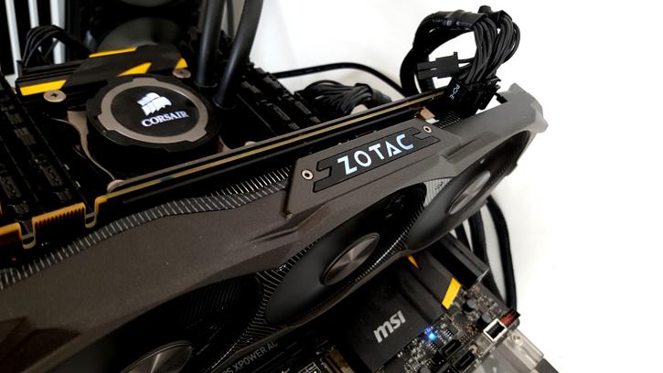
The Zotac GeForce GTX 970 runs at faster clocks; 1228 MHz GPU with a 1380 MHz Boost allowance and memory at 7.2 Gbps
