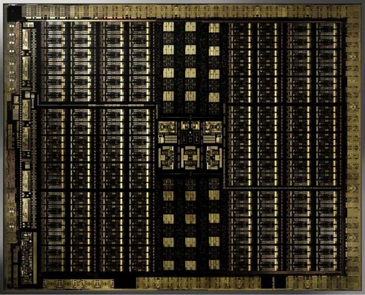
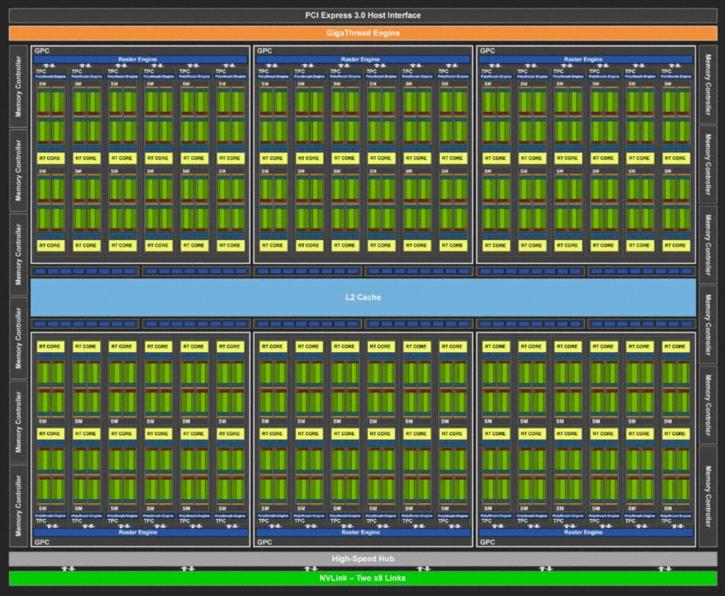
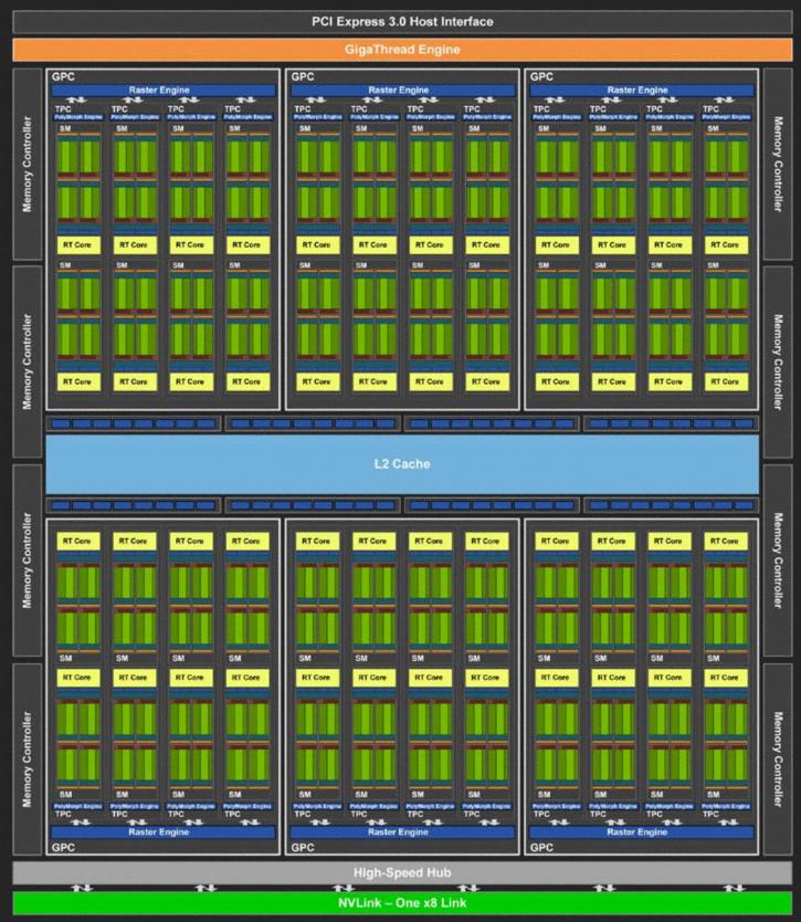
Block Diagrams TU102 104 and 106
The Turing Block Diagrams
In chapter of this architecture review, I like to chart up and present to you the separated GPU block diagrams. Mind you that the specification on the 2080 and 2080 Ti differ slightly compared to the fully enabled GPU, as the GPUs have disabled shader / RT /Tensor partitions. So the block diagrams you see here as based upon the fully enabled GPUs. Only the GeForce RTX 2070 is a fully enabled TU106 chip.
 | ||||||
|---|---|---|---|---|---|---|
| GeForce | RTX 2080 Ti FE | TU102 GPU | RTX 2080 FE | TU104 GPU | RTX 2070 FE | TU106 GPU |
| GPU | TU102 | TU102 | TU104 | TU104 | TU106 | TU106 |
| Node | TSMC 12 nm FFN | |||||
| Die Size mm² | 754 | 545 | 445 | |||
| Shader cores | 4352 | 4608 | 2944 | 3072 | 2304 | 2304 |
| Transistor count | 18.6 Billion | 18.6 Billion | 13.6 Billion | 13.6 Billion | 10.8 Billion | 10.8 Billion |
| Base frequency | 1350 MHz | 1515 MHz | 1410 MHz | |||
| Boost frequency | 1635 MHz | 1800 MHz | 1710 MHz | |||
| Memory | 11GB GDDR6 | 12GB GDDR6 | 8GB GDDR6 | 8GB GDDR6 | 8GB GDDR6 | 8GB GDDR6 |
| Memory frequency | 14 Gbps | 14 Gbps | 14 Gbps | 14 Gbps | 14 Gbps | 14 Gbps |
| Memory bus | 352-bit | 384-bit | 256-bit | 256-bit | 256-bit | 256-bit |
| Memory bandwidth | 616 GB/s | 672 GB/s | 448 GB/s | 448 GB/s | 448 GB/s | 448 GB/s |
| RT cores | 68 | 72 | 46 | 48 | 36 | 36 |
| Tensor cores | 544 | 576 | 368 | 384 | 288 | 288 |
| Texture units | 272 | 288 | 184 | 192 | 144 | 144 |
| ROPs | 96 | 96 | 64 | 64 | 64 | 64 |
| TDP | 260W | 225W | 185W | |||
| Power connector | 2x 8-pin | 8+6-pin | 8-pin | |||
| NVLink | Yes | Yes | Yes | Yes | No | No |
| Performance (RTX Ops) | 78T RTX-Ops | 60T RTX-Ops | 45T RTX-Ops | |||
| Performance (RT) | 10 Gigarays/s | 8 Gigarays/s | 6 Gigarays/s | |||
| TFlops fp32 | 14.2 / 13.4 | 10.6 / 10 | 7.9 / 7.5 | |||
| Max Therm degree C | 89 | 89 | 89 | |||
| price | $ 1199 | $ 799 | $ 599 | |||
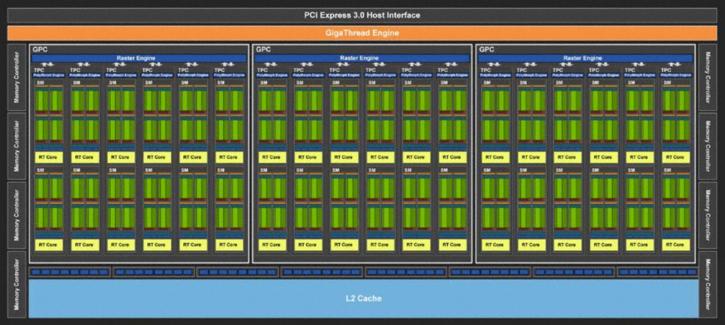
Below an overview of the official block diagram per Turing GPU:
TU102 (the base GPU GeForce RTX 2080 Ti)
TU104 (the base GPU GeForce RTX 2080)
TU106 (the base GPU GeForce RTX 2070)
