Product Teardown
Teardown
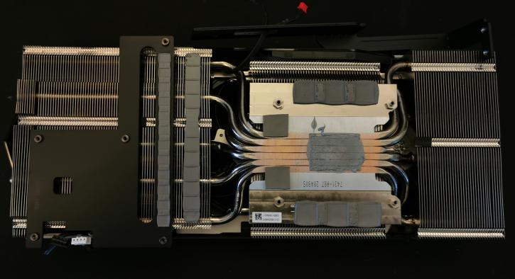
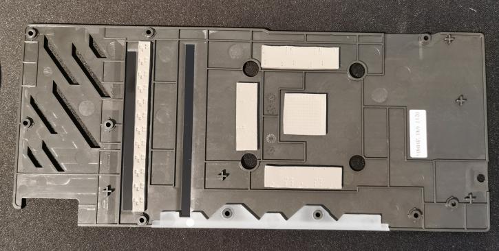
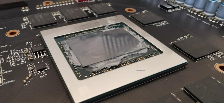
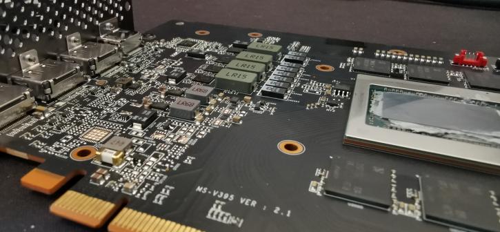
It is a request that is getting more and more daunting as we do not want to damage products. But user request on this is clear, you like a teardown and want to look to see what is going on at the PCB level. Opening up that trunk reveals a massive cooler. Nice to see are thermal padding everywhere and additional heatsinks in place at crucial segments. This also makes the card more sturdy, preventing it from bending. The backplate also reveals loads of thermal pads, helping cool down critical elements a bit. You'll notice that at that backside, for example, the GPU and GDDR6 IC locations are padded as well as part of the VRM.
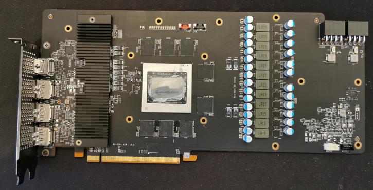
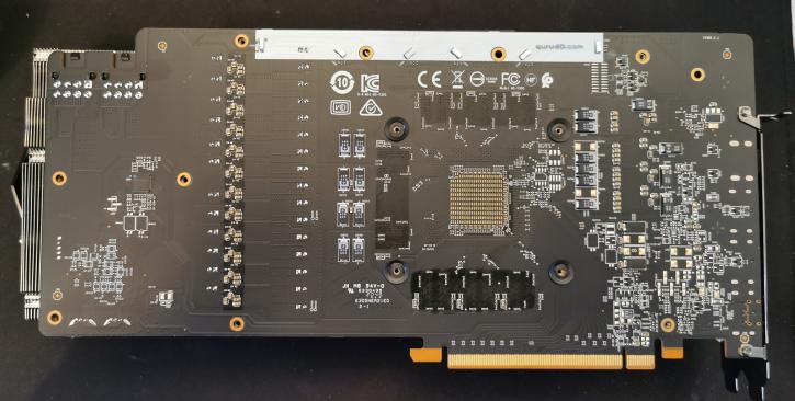
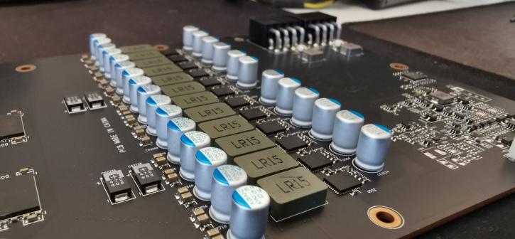
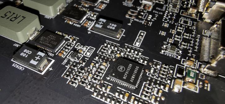
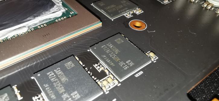
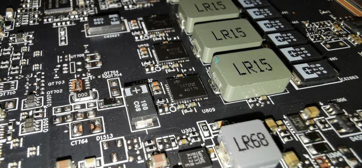
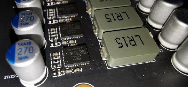
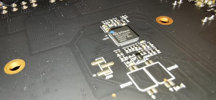
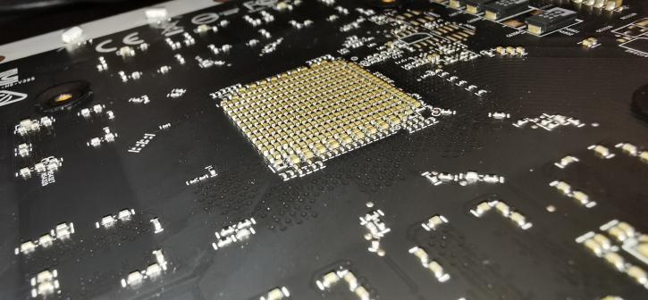
Power phases are setup as 13+3. The GPU voltage management is based on a 13 phase design powered by an Infineon XDPE132G5D controller. Looking closer at the photos, you'll notice that International Rectifier TDA21472 DrMOS ICs are used throughout the card. The memory subsystem makes use of a three-phase power configuration managed by an OnSemi NCP81022N controller. The GDDR6 chips register back as made by Samsung, qualified and validated to run 16 Gbps. Cooler LEDs these days are built onto the PCB. Highlighted at that white tripe. White paint is used here for reflection of light, of course. Yeah, MSI thought that through well. One last remark, look how gobsmacked clean that PCB looks especially at GPU and GDDR6 location. Impressive eh? I know, I am a sheer g33k, of course.