Page 2
Inside the graphics core
So here we meet again. Welcome .. let's chat a little about the G71. What's G71 you ask ? This is the codename of the chip from it's development stages. Most of you figured we'd see a 32 pixel pipeline product today. And yeah .. I was hoping it also but perhaps we have been a little to ambitious in our thinking. We'll likely have to wait on the G80 silicon for that. None the less this product is screamingly fast though.
So in essence there are three factors changed on the G71 versus G70. A smaller fabrication process at 90nm, a higher core clockspeed and of course faster memory bandwidth. That G71 chip is different though, as the transistor count went down. The 7800 GTX for example has 304 million transistors where the new 7900 GTX has 278 Million so there are differences for sure. Now we haven't received the whitepapers just yet and I unfortunately had to miss out on an NVIDIA product briefing, but word is that the new chip is based on 48 ALUs. The G71 has been manufactured at NVIDIA's latest 90nm fabrication process. Smaller fabrication processes of course offer several advantages. You could push more transistors on the GPU as you have more space to work with, but another nice advantage is a smaller chip design. That means you need to cram in less voltage into the silicon and that saves on heat. Less heat means higher clockspeeds and that's why today's product is clock roughly 100 MHz faster then it's predecessor the 7800 GTX 512MB. Did you know that the 256MB version is clocked at 430 MHz ? You can smell the performance there huh ? Really it's not all about clock for clock performance .. but it can surely help :)
Since we are on the topic of the graphics core, inside it there are precisely eight vertex units active. Also the number of pixel pipelines are identical to the 7800 GTX, there are twenty-four of them. Let me enlighten briefly what happens in the pixel pipeline for you to understand its importance. Each pixel that is rendered on your screen goes through a pipe where it'll receive its complex color/effect etc. Each time that pixel is altered it'll pass through the pixel pipeline, one pass is one clock cycle.
The 7800 GTX throughout the Series 7800+ line has had eight ROPs. ROP is short for Raster OPeration and a portion of a pipeline, responsible for AA, Blending and Z-Buffer compression. Simply stated a ROP is basically the output engine of a pixel shader pipeline. The pipeline is scalable, each pipe is available at any time in sets of 4, which we call quads.
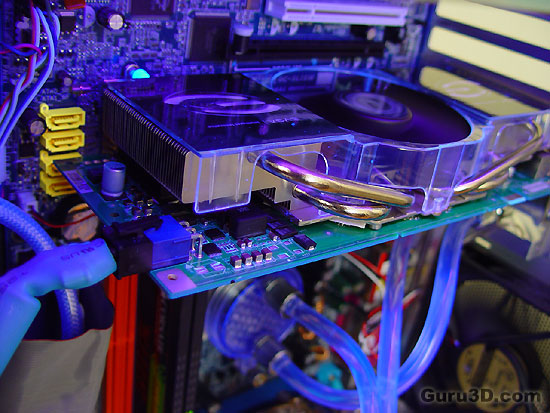
Of course next to the GPU the most important thing is it's memory to work in. We call this the framebuffer, and the faster it is the higher your memory bandwidth to work in will be. Suffice to say is that the 7900 GTX 512MB is armed with the latest and fastest memory available ... the eVGA version comes with a clock of 1760 MHz .. and that's a lot of bandwidth for sure.
Please focus on the chart below where I cite the more important specs.
|
NVIDIA GeForce 6 & 7 Product Lineup Specifications |
Product Name
# pixel processors
# vertex processors
Bus width
Memory Type/Amount
GPU Speed
RAM Speed
GeForce 7900 GTX 24 8 256-bit GDDR3/512MB 650-700MHz 1600 MHzGeForce 7900 GT 24 8 256-bit GDDR3/256MB 450MHz 1320 MHzGeForce 7800 GTX 24 8 256-bit GDDR3/512MB 560MHz 1600 MHz GeForce 7800 GTX 24 8 256-bit GDDR3/256MB 430MHz 1200MHzGeForce 7800 GT 20 7 256-bit GDDR3/256MB 400MHz 1000MHzGeForce 7800 GS 16 6 256-bit GDDR3/256MB 375MHz 1200MHz GeForce 7600 GT 12 5 128-bit GDDR3/256MB 560MHz 1400MHzGeForce 6800 Ultra **
16
6
256-bit
GDDR3/256MB
400MHz
1100MHz
GeForce 6800 GT
16
6
256-bit
GDDR3/256MB
350MHz
1000MHz
GeForce 6800 GS PCX 12 5 256-bit GDDR3/128/256MB 425MHz 1000MHzGeForce 6800 GS AGP 12 5 256-bit GDDR3/128/256MB 350MHz 1000MHzGeForce 6800
12
5
256-bit
GDDR/128MB
325MHz
700MHz
GeForce 6800 LE
8
4
256-bit
GDDR/128MB
320MHz
700MHz
GeForce 6600 GT 8 3 128-bit GDDR3/128/256MB 500MHz 1000MHzGeForce 6600 8 3 128-bit GDDR/128MB 300MHz 275(550) GeForce 6200 4 3 64/128-bit GDDR/128MB/256MB 300MHz 275(550)** Not manufactured anymore - Spec are reference specification. Speeds can differ per model and manufacturer
In many ways the product is feature wise 100% similar to the entire 7800 series. This means you'll be able to select resolutions up-to a fantastic 2560x1600 (and actually play games at that resolution) thanks to the dual link DVI connectors.
What is a shader ? What do we need to render a three dimensional object; 2D on your monitor? We start off by building some sort of structure that has a surface, that surface is being built from triangles and why triangles? They are quick to calculate. How's each triangle being processed? Each triangle has to be transformed according to its relative position and orientation to the viewer. Each of the three vertices the triangle is made up of is transformed to its proper view space position. The next step is to light the triangle by taking the transformed vertices and applying a lighting calculation for every light defined in the scene. At last the triangle needs to be projected to the screen in order to rasterize it. During rasterization the triangle will be shaded and textured.
