
What are memory timings?
When it comes to memory timings, there are a few key factors to understand. One of the most important is latency, which refers to the amount of time it takes for a request to be processed and the data to be written or read from memory. In other words, latency is like the wait time between ordering a meal at a restaurant and receiving it. The lower the latency, the faster the data can be accessed, much like how a quick meal service is preferable. Latency - lower is better.
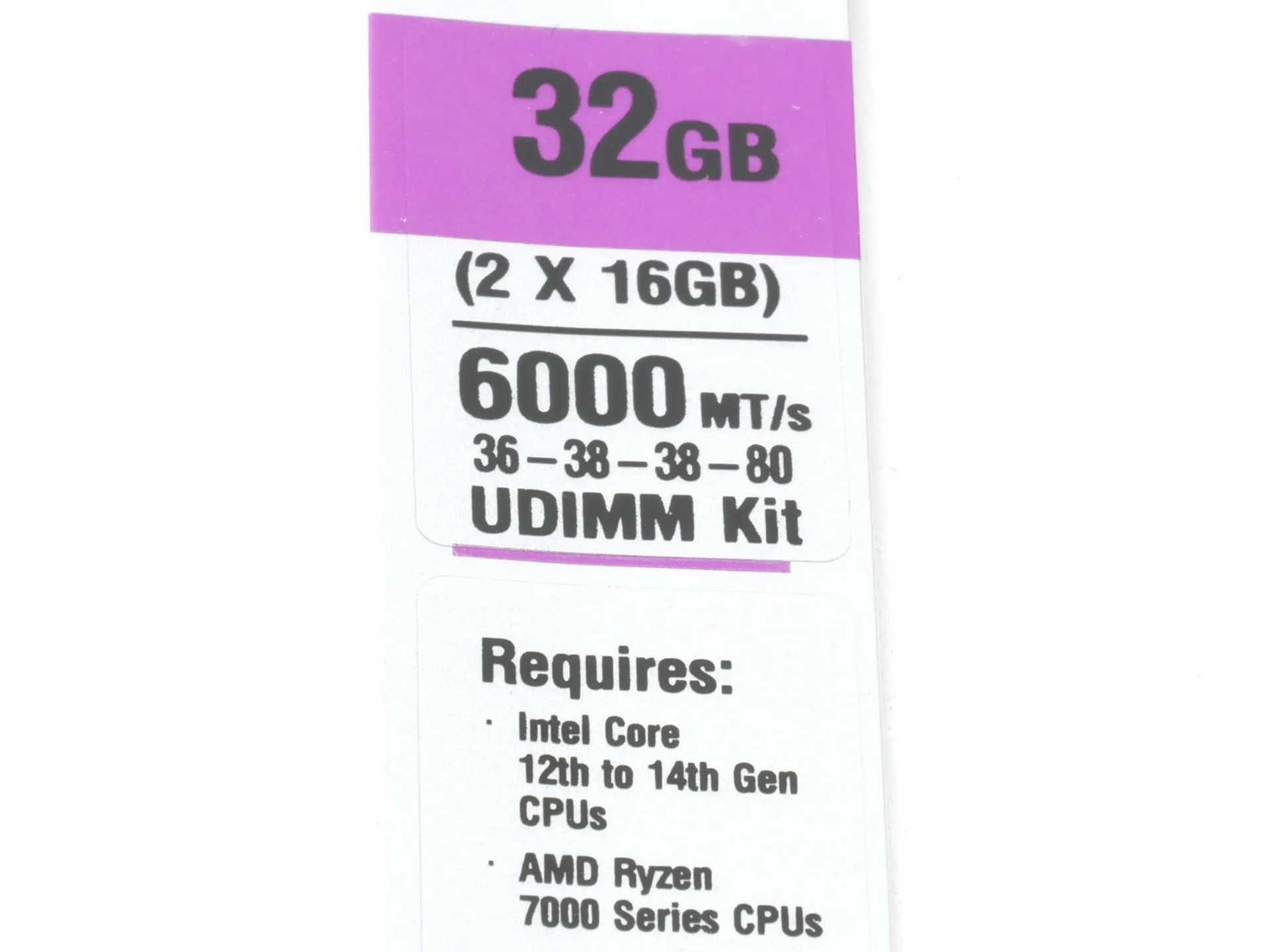
Say we notice on the packaging is this: 36-38-38-80 at 1.3 Volts for a memory kit. What do the numbers mean? Well, this refers to CAS-tRCD-tRP-tRAS CMD (respectively), and these values are measured in clock cycles.
| [ DIMMA1: Crucial CP16G60C36U5B.M8D1 ] | |||||
| Memory Module Properties: | |||||
| Module Name | Crucial CP16G60C36U5B.M8D1 | ||||
| Serial Number | E85D8E38h (948854248) | ||||
| Manufacture Date | Week 4 / 2024 | ||||
| Module Size | 16 GB (32 banks) | ||||
| Module Type | Unbuffered DIMM | ||||
| Memory Type | DDR5 SDRAM | ||||
| Memory Speed (EXPO) | DDR5-6000 (3000 MHz) | ||||
| Memory Speed | DDR5-5600 (2800 MHz) | ||||
| Module Width | 64 bit | ||||
| Module Voltage (EXPO) | 1.35 V | ||||
| Module Voltage (VDD) | 1.1 V | ||||
| Module Voltage (VDDQ) | 1.1 V | ||||
| Module Voltage (VPP) | 1.8 V | ||||
| Error Detection Method | None | ||||
| DRAM Manufacturer | Micron | ||||
| DRAM Stepping | 44h | ||||
| SDRAM Die Count | 1 | ||||
| Memory Timings: | |||||
| @ 3003 MHz (EXPO) | 36-38-38-80 (CL-RCD-RP-RAS) | ||||
| @ 2801 MHz | 50-45-45-90 (CL-RCD-RP-RAS) / 135-827-449-365-85 (RC-RFC1-RFC2-RFCSB-WR) | ||||
| @ 2801 MHz | 46-45-45-90 (CL-RCD-RP-RAS) / 135-827-449-365-85 (RC-RFC1-RFC2-RFCSB-WR) | ||||
| @ 2625 MHz | 42-42-42-84 (CL-RCD-RP-RAS) / 126-775-420-342-79 (RC-RFC1-RFC2-RFCSB-WR) | ||||
| @ 2500 MHz | 40-40-40-80 (CL-RCD-RP-RAS) / 120-738-400-325-75 (RC-RFC1-RFC2-RFCSB-WR) | ||||
| @ 2250 MHz | 36-36-36-72 (CL-RCD-RP-RAS) / 108-664-360-293-68 (RC-RFC1-RFC2-RFCSB-WR) | ||||
| @ 2000 MHz | 32-32-32-64 (CL-RCD-RP-RAS) / 96-590-320-260-60 (RC-RFC1-RFC2-RFCSB-WR) | ||||
| @ 1875 MHz | 30-30-30-60 (CL-RCD-RP-RAS) / 90-554-300-244-57 (RC-RFC1-RFC2-RFCSB-WR) | ||||
| @ 1750 MHz | 28-28-28-56 (CL-RCD-RP-RAS) / 84-517-280-228-53 (RC-RFC1-RFC2-RFCSB-WR) | ||||
| @ 1624 MHz | 26-26-26-52 (CL-RCD-RP-RAS) / 78-480-260-212-49 (RC-RFC1-RFC2-RFCSB-WR) | ||||
| @ 1374 MHz | 22-22-22-44 (CL-RCD-RP-RAS) / 66-406-220-179-42 (RC-RFC1-RFC2-RFCSB-WR) | ||||
| Extreme Memory Profile v3.0: | |||||
| Profile Name | 6000 CL36 | ||||
| Voltage (VDD) | 0.00 V | ||||
| Voltage (VDDQ) | 2.100 V | ||||
| Voltage (VPP) | 0.00 V | ||||
| Voltage (Memory Controller) | 0.00 V | ||||
| Recommended DIMMs Per Channel | 1 | ||||
| Dynamic Memory Boost | Not Supported | ||||
| Real-Time Memory Frequency Overclocking | Not Supported | ||||
| @ 28 MHz | 90-1-2-1 (CL-RCD-RP-RAS) / 1-30-216-1-2 (RC-RFC1-RFC2-RFCSB-WR) | ||||
| @ 28 MHz | 76-1-2-1 (CL-RCD-RP-RAS) / 1-30-216-1-2 (RC-RFC1-RFC2-RFCSB-WR) | ||||
| @ 28 MHz | 70-1-2-1 (CL-RCD-RP-RAS) / 1-30-216-1-2 (RC-RFC1-RFC2-RFCSB-WR) | ||||
| @ 28 MHz | 68-1-2-1 (CL-RCD-RP-RAS) / 1-30-216-1-2 (RC-RFC1-RFC2-RFCSB-WR) | ||||
| @ 28 MHz | 66-1-2-1 (CL-RCD-RP-RAS) / 1-30-216-1-2 (RC-RFC1-RFC2-RFCSB-WR) | ||||
| @ 28 MHz | 58-1-2-1 (CL-RCD-RP-RAS) / 1-30-216-1-2 (RC-RFC1-RFC2-RFCSB-WR) | ||||
| @ 28 MHz | 42-1-2-1 (CL-RCD-RP-RAS) / 1-30-216-1-2 (RC-RFC1-RFC2-RFCSB-WR) | ||||
| @ 28 MHz | 28-1-2-1 (CL-RCD-RP-RAS) / 1-30-216-1-2 (RC-RFC1-RFC2-RFCSB-WR) | ||||
| @ 28 MHz | 22-1-2-1 (CL-RCD-RP-RAS) / 1-30-216-1-2 (RC-RFC1-RFC2-RFCSB-WR) | ||||
| @ 28 MHz | 20-1-2-1 (CL-RCD-RP-RAS) / 1-30-216-1-2 (RC-RFC1-RFC2-RFCSB-WR) | ||||
| Extreme Memory Profile v3.0: | |||||
| Profile Name | 5600 CL36 | ||||
| Memory Speed | DDR5-5600 (2800 MHz) | ||||
| Voltage (VDD) | 1.25 V | ||||
| Voltage (VDDQ) | 1.25 V | ||||
| Voltage (VPP) | 1.80 V | ||||
| Voltage (Memory Controller) | 3.155 V | ||||
| Recommended DIMMs Per Channel | 1 | ||||
| Dynamic Memory Boost | Not Supported | ||||
| Real-Time Memory Frequency Overclocking | Not Supported | ||||
| @ 2801 MHz | 42-38-38-80 (CL-RCD-RP-RAS) / 118-827-449-365-85 (RC-RFC1-RFC2-RFCSB-WR) | ||||
| @ 2801 MHz | 40-38-38-80 (CL-RCD-RP-RAS) / 118-827-449-365-85 (RC-RFC1-RFC2-RFCSB-WR) | ||||
| @ 2801 MHz | 38-38-38-80 (CL-RCD-RP-RAS) / 118-827-449-365-85 (RC-RFC1-RFC2-RFCSB-WR) | ||||
| @ 2801 MHz | 36-38-38-80 (CL-RCD-RP-RAS) / 118-827-449-365-85 (RC-RFC1-RFC2-RFCSB-WR) | ||||
| @ 2489 MHz | 32-34-34-72 (CL-RCD-RP-RAS) / 105-735-399-324-75 (RC-RFC1-RFC2-RFCSB-WR) | ||||
| @ 2334 MHz | 30-32-32-67 (CL-RCD-RP-RAS) / 99-689-374-304-71 (RC-RFC1-RFC2-RFCSB-WR) | ||||
| @ 2178 MHz | 28-30-30-63 (CL-RCD-RP-RAS) / 92-643-349-284-66 (RC-RFC1-RFC2-RFCSB-WR) | ||||
| @ 2023 MHz | 26-28-28-58 (CL-RCD-RP-RAS) / 86-597-324-263-61 (RC-RFC1-RFC2-RFCSB-WR) | ||||
| @ 1711 MHz | 22-24-24-49 (CL-RCD-RP-RAS) / 73-505-274-223-52 (RC-RFC1-RFC2-RFCSB-WR) | ||||
| EXtended Profiles for Overclocking v1.0: | |||||
| Memory Speed | DDR5-6000 (3000 MHz) | ||||
| Voltage (VDD) | 1.35 V | ||||
| Voltage (VDDQ) | 1.35 V | ||||
| Voltage (VPP) | 1.80 V | ||||
| Recommended DIMMs Per Channel | 1 | ||||
| Memory Timings | 36-38-38-80 (CL-RCD-RP-RAS) / 118-886-481-391-91 (RC-RFC1-RFC2-RFCSB-WR) | ||||
| EXtended Profiles for Overclocking v1.0: | |||||
| Memory Speed | DDR5-5600 (2800 MHz) | ||||
| Voltage (VDD) | 1.25 V | ||||
| Voltage (VDDQ) | 1.25 V | ||||
| Voltage (VPP) | 1.80 V | ||||
| Recommended DIMMs Per Channel | 1 | ||||
| Memory Timings | 36-38-38-80 (CL-RCD-RP-RAS) / 118-827-449-365-85 (RC-RFC1-RFC2-RFCSB-WR) | ||||
| Memory Module Features: | |||||
| Asymmetrical Module | No | ||||
| HeatSpreader | Not Present | ||||
| Memory Module Manufacturer: | |||||
| Company Name | Micron Technology, Inc. | ||||
CAS Latency
Undoubtedly, one of the most essential timings is that of the CAS Latency and is also the one most people can actually understand. Since data is often accessed sequentially (same row), the CPU only needs to select the next column in the row to get the next piece of data. In other words, CAS Latency is the delay between the CAS signal and the availability of valid data on the data pins (DQ). Therefore, the latency between column accesses (CAS), plays an important role in the performance of the memory. The lower the latency, the better the performance. However, the memory modules must be capable of supporting low latency settings.
tRCD
There is a delay from when a row is activated to when the cell (or column) is activated via the CAS signal and data can be written to or read from a memory cell. This delay is called tRCD. When memory is accessed sequentially, the row is already active and tRCD will not have much impact. However, if memory is not accessed in a linear fashion, the current active row must be deactivated and then a new row selected/activated. It is this example where low tRCD's can improve performance. However, like any other memory timing, putting this too low for the module can result in instability.
tRP
tRP is the time required to terminate one Row access and begin the next row access. Another way to look at this it that tRP is the delay required between deactivating the current row and selecting the next row. Therefore, in conjunction with tRCD, the time required (or clock cycles required) to switch banks (or rows) and select the next cell for either reading, writing or refreshing is a combination of tRP and tRCD.
tRAS
Memory architecture is like a spreadsheet with row upon row and column upon column with each row being 1 bank. In order for the CPU to access memory, it must first determine which Row or Bank in the memory that is to be accessed and activate that row via the RAS signal. Once activated, the row can be accessed over and over until the data is exhausted. This is why tRAS has little effect on overall system performance but could impact system stability if set incorrectly.
Command Rate
The Command Rate is the time needed between the chip select signal and when commands can be issued to the RAM module IC.
