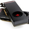
Product Innards
Product Innards
So, we take off the back-plate locked in with screws. At the backside there is a gap between the components and back-plate through the use of riser standoffs. Let's immediately zoom in at the front-side, as that's the sugah-shot right there :)
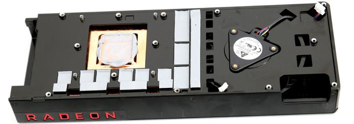
The cooling solution, it uses heat-pipes that pass through a copper block, with thermal paste tied to the all-copper yet nickel plated block. That's as good as it gets really. When we flip the PCB it around you can also see that the critical components are covered with a full contact plate (padding underneath as well). The power stages have padding and thus is cooled as well as most ICs.
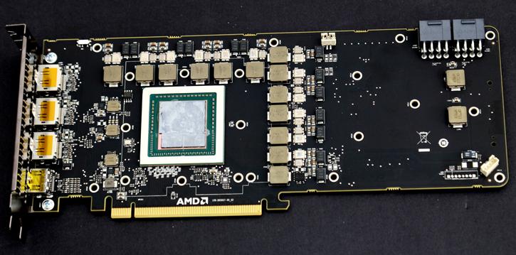
With the heatplate removed we now have the full PCB and all comonents visible. This is a very clean PCB design alright, that right side hardly is used other then to provide a more sturdy design for the cooler. Let's run through some of the components.
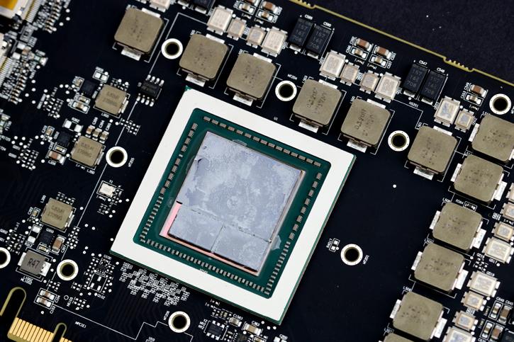
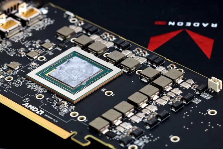
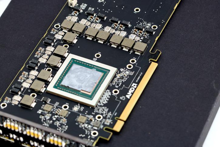
First and foremost, here we have the Vega 10 graphics processor from AMD with its 4096 Shader Cores. I left the thermal compound in there as I need to re-assemble the card fast for further testing. The PCB and GPU design is the same for both the 56 and 64 models btw. At the lower GPU side you can see the two HBM2 stacks, each 4 GB.
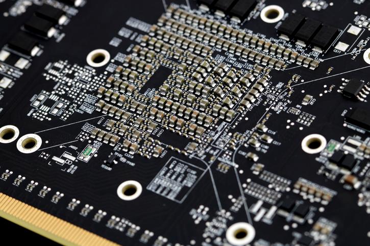
So in the above photo you can see the opposing backside of the GPU, it shows many, really many ceramic capacitors ..
The card uses solid capacitors that are surrounding the GPU socket. We'll look at the voltage regulator in a second as well. No memory leaves open opportunities in terms of placement on the PCB. As such you can see, voltage regulators are located at what normally would be the location of the memory ICs. You might think 12, but you are looking at a 6+1-phase design for power delivery to the GPU and HBM2. I'll explain after the next photo.
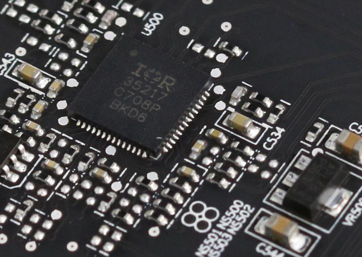
The reference design is using a International Rectifier IR35217 power controller, a fairy undocumented 8-channel multi-phase controller that can provide six phases for the GPU and another two for say memory. If you look at the previous image you'll notice AMD is doubling GPU phases up, they in fact use six IR 3598 phase doublers located at the backside of the PCB. This is common on many graphics cards. So it's 6 phases, but doubled up to 12.
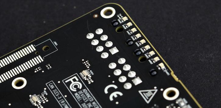
Last photo at the top side the power load indicator, aka cluster of LEDs, configurable in either blue or red.
