Page One - Inside NVIDIA
Back in May, I visited NVIDIA's HQ in San Francisco Santa Clara. Although security was raised at that point due to some smaller incidents we where allowed to take some photo's inside the complex. .. It was probably one of the most coolest thing most of us ever saw this year as such an opportuni ty is rare. Last week I was going through some photos and figured that this not publishing the photo's would be a true waste.The tour was actually guided by an ex-Matrox PR employee that I knew, Diane Vanesse. As stated security was extremely tight due to that incident and we where told we would not be allowed to make any photo's inside the NVIDIA premises. Let me start off with a little story. During a break we were outside the building and started taking some photos as we refused to go back empty handed. After a minute or two, a security guard ran towards us, and forced us not to make any photos. Even when we walked to the open road on non-NVIDIA owned ground, the man would do anything to block my camera.
Anyway, we took that man inside and started ranting a little to our PR managers. I think it was Dan Vivoli who gave the final okay sign so we could at least take some photo's outside the buildings.
So that was essentially very bad news for an inside tour of the building. Why did all this happen, why was everything so tight ? This was the deal, a few weeks before our visit a journalist took images of something he should not have and published it. I guess at that time it was the NV35 that went public while all information regarding it was still disclosed. At that time the call was made not to allow people to take photos inside and outside the building. The minute we heard that everybody's face got .. well very sour. I think Andrew Humber and Adam Foat came to the rescue here .. they went upstairs and came back with the good news. We where allowed to make a few photo's inside the complex. I probably made 200 photos of which I made a small selection that I think are suitable for publishing on-line.
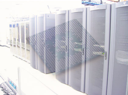
That day was of course filled with meetings, information and technology briefing yet we'll focus on the tour in this article. In the tour we saw the a lot of stuff, it was really amazing. I mean one of the first stops was at the NVIDIA server farm. I figured Guru3D.com is big, as it makes use of 4 servers (soon 5). Well, take a look at the images on the next pages, it's basically shock and awe. The computational power to emulate, simulate and store a chip-design goes beyond comprehension.
We saw a lot of stuff really, server park, hardware quality testing laboratory, and even the holiest of holy (why does pulp fiction always comes to mind) the lab with the multi-million dollar equipment where they check the cores to the transistor precisely with huge ion ray microscopes. So cool.
Of course many departments we can't show you. These departments included shipping and receiving, technology laboratories where they dissect the NVxx'es, quality labs, research labs with scanning tunnel microscopes that scan up-to the nanometer as we weren't allowed to take photos.
The next pages will have photos primarily as this is a pictorial to show you what exactly is going on inside NVIDIA. All the technology that is being used in there I could not even explain even if I wanted to. All in all, a very impressive day.
Understand that some photos have been edited by us as they contained some sensitive information like IP's and stuff which was blurred out. Let's get started with an overview of the buildings.