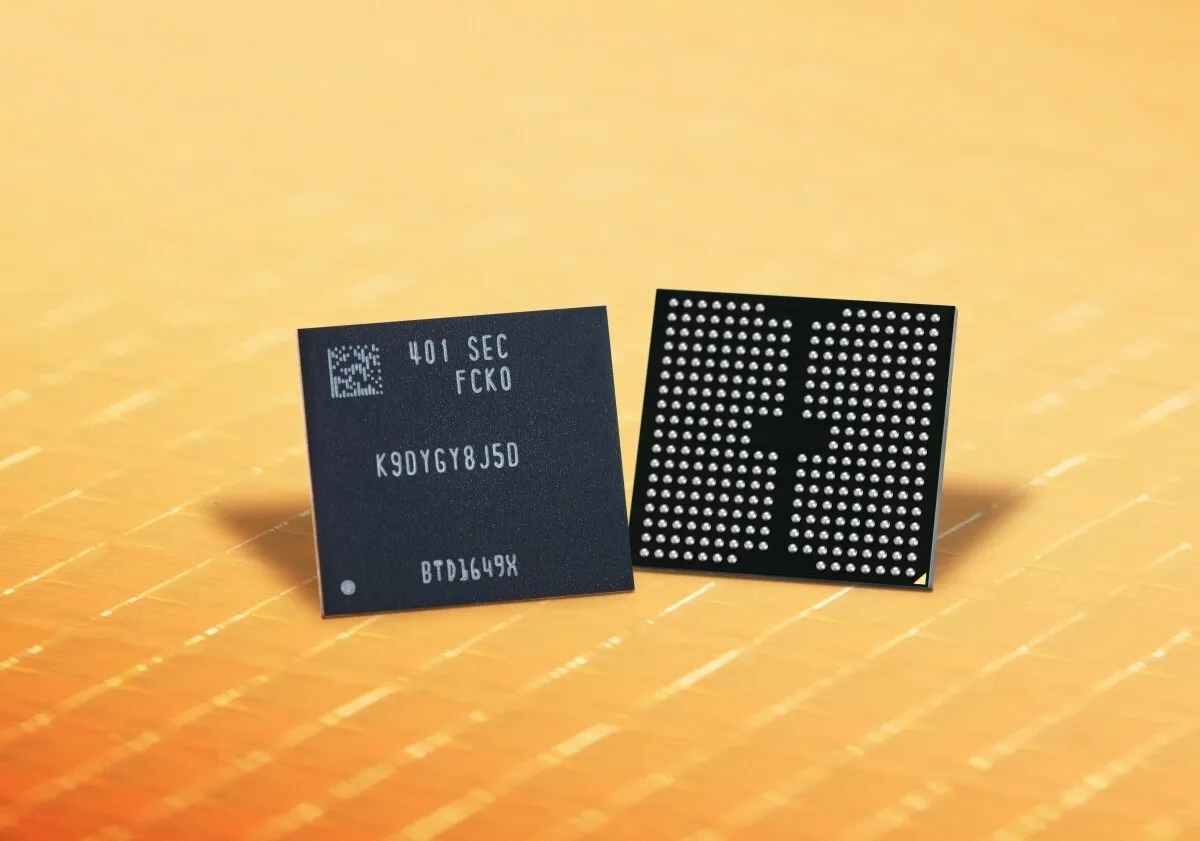
The company has achieved approximately a 50% increase in bit density over the previous 8th-generation V-NAND, facilitated by the smallest cell size yet and the thinnest mold in the industry. Samsung's proprietary "channel hole etching" technology, which enables the drilling of cell layers in a double-stack structure, is critical in this advancement, allowing for higher layer counts and more efficient fabrication.
The 9th-generation V-NAND also introduces the Toggle 5.1 NAND flash interface, which enhances data transfer speeds by 33% to 3.2 gigabits-per-second (Gbps). This interface, combined with planned support for PCIe 5.0, aims to bolster Samsung's presence in the high-performance solid-state drive (SSD) market. In line with global sustainability goals, the new V-NAND design improves power efficiency by 10% over previous generations. This advancement aligns with growing consumer demand for reduced energy consumption and lower carbon emissions. Samsung's production of the 1Tb TLC V-NAND commenced this month, with a quad-level cell (QLC) variant expected to follow in the latter half of the year.