In a keynote address, leading vendor Micron Technology (Micron) discussed scaling techniques for 3D NAND flash technology. Stacking memory cells perpendicular to the surface of the silicon wafer is the most efficient approach to improving the density and capacity of 3D NAND flash.
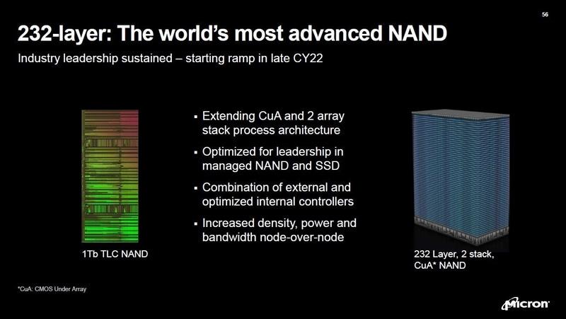
Micron has created and mass-produced 176-layer 3D NAND flash with a huge number of stacked cells. Moreover, on May 12, 2022, just prior to IMW 2022, the company stated to investors during a briefing session that it has created 232-layer 3D NAND flash technology. Based on a straightforward calculation, the memory density is 1.32 times that of 176 layers. The investor briefing slide depicted a TLC (3bit / cell) technique 1Tbit die picture. In addition, although not published in the IMW 2022 publication, the investor briefing slide was displayed during the keynote address.
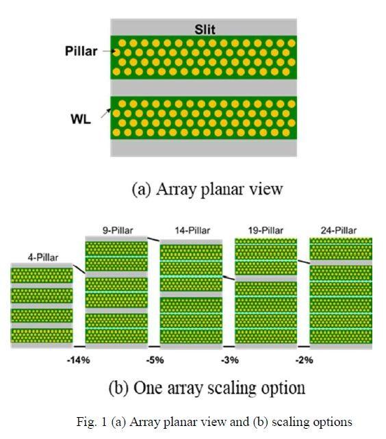
Compared to stacking in the vertical direction (Z direction), densification is slower parallel to the silicon wafer surface (horizontal direction or XY direction). However, attempts are being undertaken to enhance the density by increasing the distance between sacrificial etching grooves. In the past, grooves were supplied for each of the four channels (pillars), however for each of the nine channels, this was changed. Consequently, the density is enhanced by 14 percent. However, if the number is greater than nine, the groove spacing can be widened without a significant increase in density.
An effort to improve the density by increasing the interval between sacrificial etching groove insertions. According to a report released by Micron Technology in IMW 2022, there are also efforts to reduce the channel width and channel pitch in order to boost the density. This method necessitates advancements in lithography and etching, although the density increase is minimal. Increasing the number of memory cells stacked vertically complicates channel etching. Therefore, an effort is made to limit the height growth by thinning each layer (tier). Nevertheless, thinning the tier increases the parasitic resistance and capacitance of the word line, which slows down write and read operations. Even more dangerous, if it is built too thin, the electrical interference between neighboring cells will be too great to ignore.
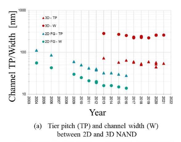
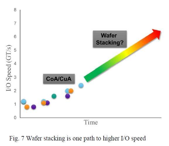
Variations in 2D NAND flash and 3D NAND flash channel tier pitch (TP) and channel width (W). From a study published in IMW 2022 by Micron Technology (Paper No. 1.1) In addition, Micron offered opportunities to increase input and output speeds. In 3D NAND flash, techniques for increasing storage density by monolithically stacking CMOS logic peripheral circuits and memory cell arrays are gaining popularity. With this method, however, CMOS peripheral circuits are exposed to the memory cell array process (high temperature processing) and deteriorate, which may impede the enhancement of operating speed. Consequently, a method has been developed in which a CMOS peripheral circuit is constructed on another silicon wafer and bonded to a memory cell array wafer.
Trend of input/output speed improvement for 3D NAND memory. From a study published in IMW 2022 by Micron Technology (Paper No. 1.1) The technology required to realize 3D NAND flash will become increasingly challenging, but its boundaries have not yet been determined. Until further notice, we can anticipate an increase in memory density.
Micron Technology Talks about NAND as well, 232-layer 3D NAND flash technology inbound