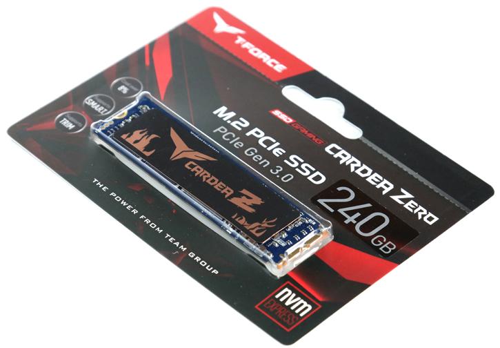
Product Showcase
Product Showcase
The following images were taken at high-resolution and then cropped and scaled down. The camera used was a Canon DSLR shooting 24 MegaPixel photos. Right then, off we go.
The sample we have at hand is the 240GB M.2 model. Performance is listed as 2,600 MB/s for reads and 1,450 MB/sec for writes with roughly 150 IOPS at 4k random writes QD32 aligned disk access with our tested model.
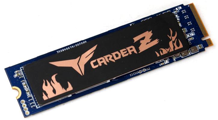
Above, the tested unit; you should easily be able to place the M.2 unit into a compatible motherboard. All Z97/X99/Z170/Z270/Z370 and AMD B350/X370/X399 motherboards support it. You should however check out with the motherboard manufacturer if you have a x4 lane PCIe version with NVMe support.
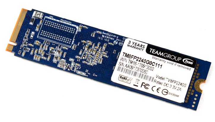
The compact M.2 2280 (2280 = 80 mm) form factor ensures compatibility with next-generation desktop and mobile platforms that support the M.2 PCIe slot and interface. The backside holds two NAND chips and an empty SMT trace for a DRAM chip (cache). There's one at the frontside though.
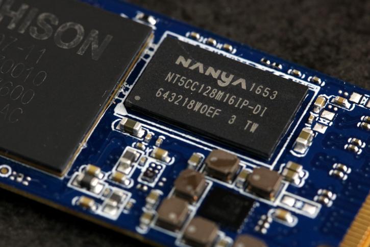
With the heatsink removed we see the top of the SSD, it also holds two NAND chips on the top side, two on the back, a Nanya DRAM cache chip (DDR3-1600 DRAM) sitting enxt to the Phison controller.
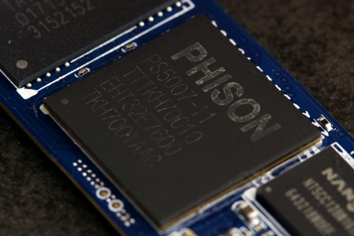
The chip read out as a Phison Series 5007-11 likely E7 NVMe controller. The one supports 15 nm SLC/MLC/TLC as well as the latest 3D (vertically stacked) NAND. These controllers support up to 2 Terabytes today and will expand to 4 Terabytes in the coming future as well as supporting NVMe L1 sub-state with less than 5 mW in L1.2 low power mode. The 480 GB configuration uses a 1,024 MB DRAM buffer that the company deploys in a single package from Nanya
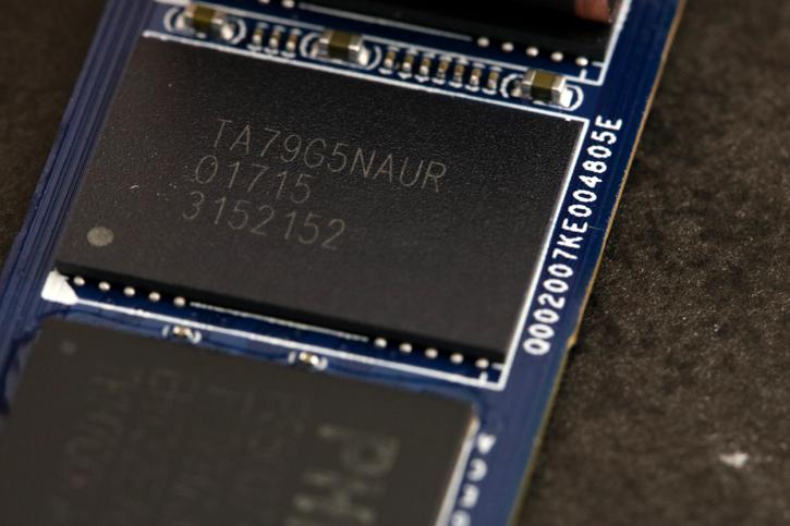
15nm MLC reveals TA79G5NAUR. That would be a single packages of 64GB x4. TA, it is a Toshiba 15nm MLC NAND flash memory. You'll find four flash NAND packages, two on each side of the PCB. Perhaps in the future a 1 TB version will be launched as the backside of the PCB reveals an empty SMT trace for another DRAM chip.
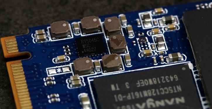
And up top a richtek power management unit slash Power solution for the SSD.
