Product Showcase
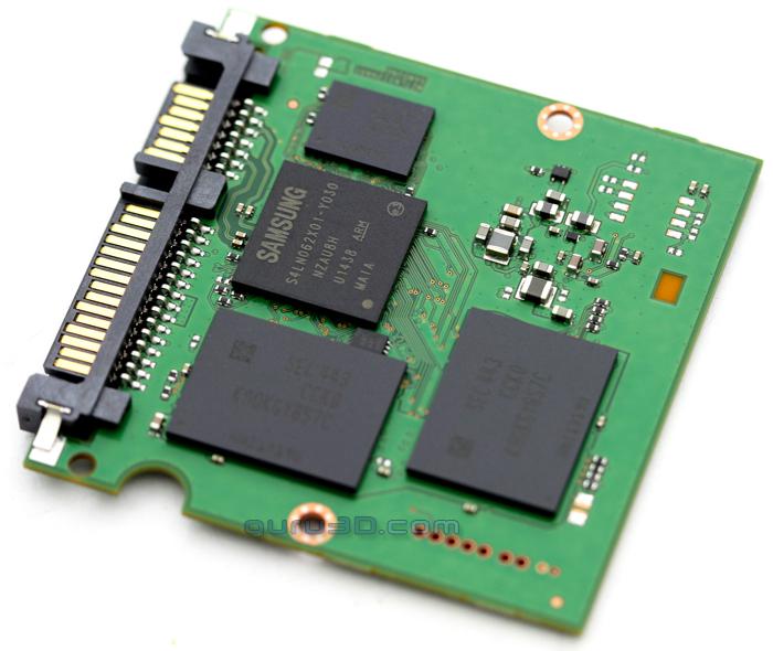
The SSD can be opened up and shows a half size PCB. This 6 Gbps storage unit makes use of Samsung's own MLC 3D-V-NAND.
A total of just four NAND flash memory ICs can be spotted on the PCB for the entire 500 GB! The NAND FLASH partitions are assigned directly to the controller. All the way to the upper left you can see two ICs, these are in fact a RAM cache IC and the controller.
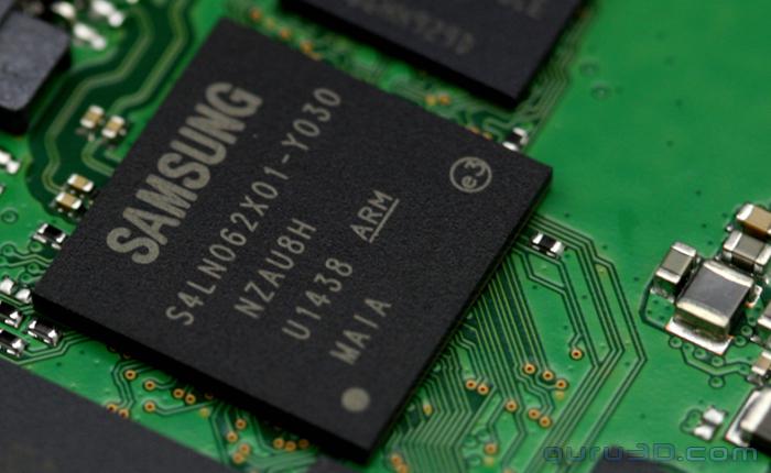
Here we can see the MGX controller. This is multi-controller with the ability of a possible 175 MB/s to 200 MB/s per channel throughput, which is a really high value yet becoming the norm for enthusiast class SSDs anno 2014.
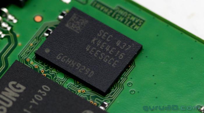
In the photo above we zoom in a little on the DDR3 memory cache chip from Samsung. This functions as cache chip/buffer.
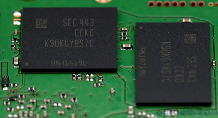
As stated, the NAND used is the new 3D V-NAND in architecture where memory celles are stacked and this way they can put more of them in a chip. These ICs are based on 32 layer 3D V-NAND. An interesting fact is that the power consumption of the Samsung SSD is extraordinary low with an IDLE rating of 2 Milli Watts and roughly 4 Watts when active. We can see these SSDs end up in both notebooks and PCs.
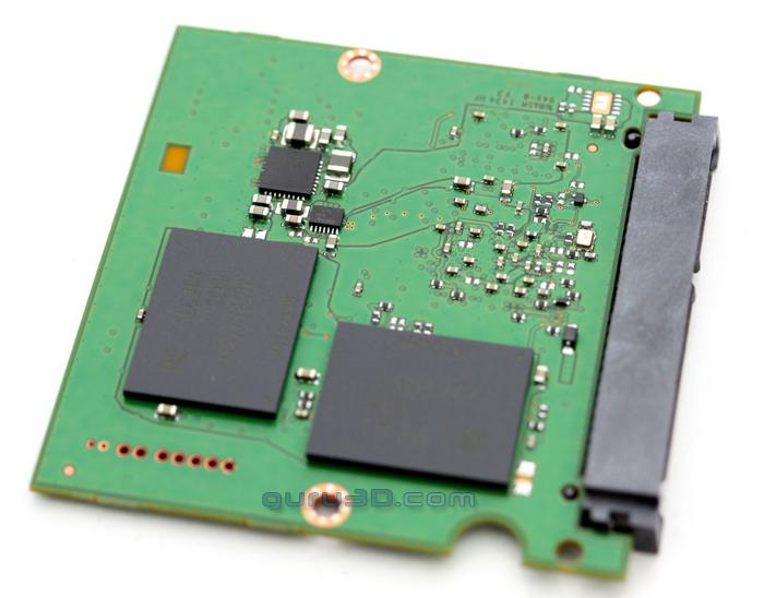
This is the backside of the PCB, very few NAND ICs, in total on both sides you will count four of them. That is the strick with 32 layer 3D V-NAND, they can stack cells and this have less chips to produce. Less components needed equals a cheaper to produce product.
