Electronics Overview
We are going to discuss the various components of the Big Joe IVs. In comparison to more traditional design class Ds are more complex in topology and design. What makes Class D so exciting to audio nuts is these amplifiers are very linear in their response and they are exceedingly efficient in comparison to other topologies that lose a great deal of power through heat.
Basically we have an ADC, a PWM controller final amp power stage. Yes, thats right there is an analog to digital converter in these amplifiers.
ADC PCM1803A
FSA used a Texas Instruments PCM1803A ADC chip for these duties. This chip takes the analog signal from the input and converts it to a PCM digital signal that will be processed in the following stage.
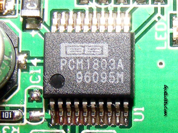
Lets take a look at the specifications of this chip:
The 1803 samples at 24/96, has a 103dB SNR, a 103dB dynamic range and a THD+N of -95dB. This ADC has single ended voltage inputs, put in simple terms it just accepts a signal and ground.
PWM Controller TAS5010
This chip is a combination of internal functions that need to be accomplished to have class D amplification. Without getting too technical, simply The TAS5010 accepts a PCM signal from the output of the ADC mentioned above and converts it to a 3.3v PWM signal internally.
The large scale PWM audio signal is outputted for the main power section below.
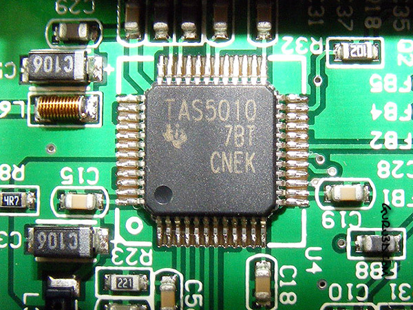
The chip offers a 96dB Dynamic range and a THD+N rating of <0.08% and has an excellent power rating of over 90%.
Power Stage TAS5121
This is where the amplifiers power comes from of 100 watts per side. The TAS5121 is a PWM input power amplifier module. Lets take a look at the specifications and a THD+N graph to get a better idea of the output characteristics.
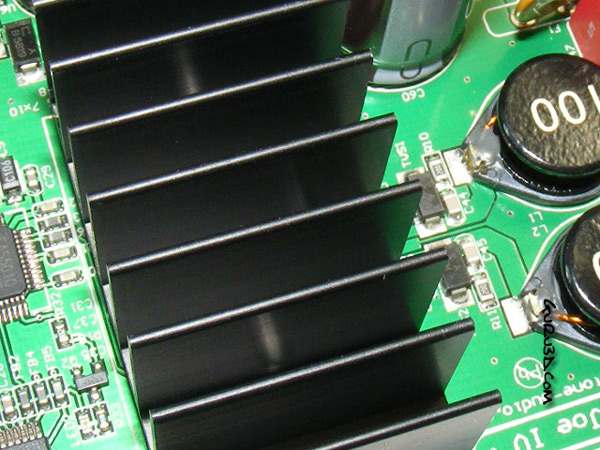
Note, internally the power amp chip has a heatsink, to prevent damage we left the unit installed.
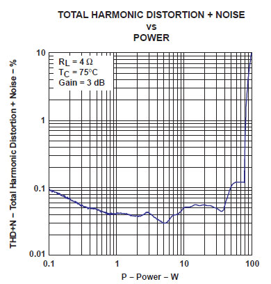
We have included the measured THD+Noise Vs. Power graph, we can see this amp provides very good measurements for distortion and noise with higher distortion ratings only coming at the highest output power levels.
