2 - Specifications, Technology
Okay then, to be able to understand eVGA nForce 750 FTW we need to explain to you what it is and what it isn't and I can do that really simple for you.
No matter how and at what angle you look at it, this mainboard is based on the nForce 780i (with an i for Intel) SLI chipset. The product is based on a 6 layer PCB; and consists of three discrete chips; the first two known as the 750i MCP and the 750i SPP, also called North and South bridge's as is more commonly accepted. The third being the tiny nForce 200 chip. The NVIDIA nForce 200 chip is nothing more than a PCI Express switch chip with one upstream port and up to four downstream ports allowing all your PCIe functionality at full or if preferred less bandwidth (4x8 PCIe lanes).
The SPP and MCP (the mainboard chipset chips) are fabricated on TSMC's 90nm process technology. The new chipset brings support for the latest Socket 775 processors from Intel:
- Quad Core Yorkfield & duo core Wolfdale (45nm Penryn)
- Current (Kentsfield) Quad core & Duo Core processors (Conroe 65nm)
- All LGA775 Pentium processors
The 750 is in fact a 780 yet with some features stripped away. The features stripped away are well .. not really needed anyway, but let's have a look and compare. We can do this pretty easily by comparing NVIDIA's internal block-diagrams of the architectural features.
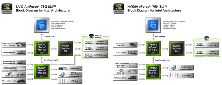
On the left side you cans ee the nForce 780i SLI - on the right the 750i SLI chipset. First thing you'll notice, 750 does not have SLI memory, meaning no automated EPP features that set timings and voltages. A loss yes, but not a biggy as you can set these timings manually. Out of the box the DDR2 memory support is 800 MHz, yet don't worry. We had Reaper memory on our board running at it's default 1148 MHz just fine, remember eVGA tweaked this mainboard for extremely high performance versus stability.
When we move downward on the block diagram we notice that the MCP is missing a couple PCIe lanes. And hey, not needed as you'll have two PCIe x16 slots, not three and thus plenty of PCIe lanes available. NVIDIA however did want to make your system PCIe 2.0 compliant, so they have inserted a bridge chip called the NV nForce 200 that is responsible for creating 2x x16 PCIe lanes fully compliant with the 2.0 standard.
The new PCie 2.0 standard, brings a boosts to the PCIe interface. The total capacity of the PCI Express 2.0 bus is now 5Gbps, twice the old standard, and an x16 connector will now be able to achieve transfers as high as 16Gbps. It is backwards compatible with PCIe 1.1 cards, making it simple for motherboard manufacturers to transition to it in the future. Cool stuff, yet it's so high-end that at this time you will just not notice a performance difference. The latest G92 graphics cards already have 2.0 compatibility though.
The rest that was stripped away is the more insignificant stuff. One GBit/s Ethernet port instead of two. 8 USB 2.0 ports instead of 10, no ESA certification. And though this one I find a bit of a lack luster, 4 SATA connectors instead of 6.
Now despite a good number of stripped away features, eVGA did it's best to compensate that by making a 100% enthusiast platform, the FTW edition. This mainboard is a good upgrade over the nForce series 6 mainboards. The industry has been moving forward and we now see slow adoption of PCIe 2.0, new Intel Penryn (45nm) Core 2 processors are slowly being released. Touching the subject of Intel's new Penryn processors. The nForce 750i SLI mainboard, as opposed to 680i, is fully compatible with the new Intel 45nm Duo & Quad core processors, but only the 1333 MHz processors are actually 'officially' supported.
But again, this is the FTW edition, if your processor can take it, you could even force a 1800 MHz FSB pretty easily. That is just no limit .. this is the stuff the mainboard was designed for. As our overclock chapter will show you, we even overclocked a 2400 MHz Core 2 Quad processor Q6600 (2400 MHz) towards 3600 MHz in less than 10 seconds.