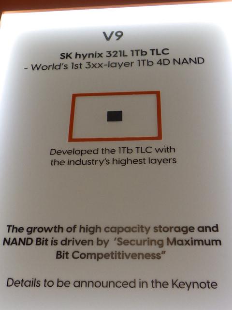
The Flash Memory Summit (FMS), a distinguished event centered on NAND flash memory and its applications, occurred on August 7. An outstanding innovation highlighted at the summit was SK hynix's 4D V9 technology, an advanced 3D NAND flash technology.
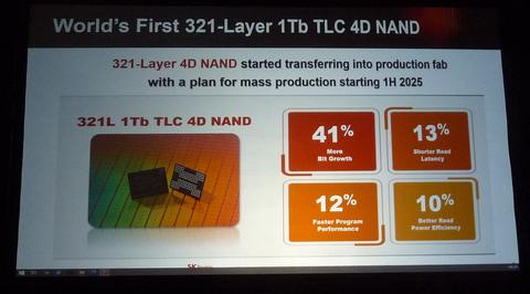
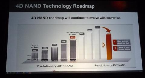
This groundbreaking design incorporates an impressive 321 layers of memory cells, delivering a storage capacity of 1Tbit per silicon die while utilizing a 3-bit/cell (TLC) multilevel storage approach. In comparison to the preceding 4D V8 generation with 238 layers, the 321-layer design signifies a 35% advancement. This enhanced version offers a 41% increase in storage density, 13% lower read latency, 12% higher write throughput, and 10% lower read power consumption compared to its predecessor.
PC Watch Japan reported a program throughput of 194 MB/s for a new NAND Flash technology. This represents a notable 26 MB/s improvement over the previous SK Hynix 176-layer NAND variant. Notably, this achievement marks the highest reported program throughput among all publicly announced NAND Flash solutions.
Interestingly, Kioxia, a key player in the field, is poised to exceed this milestone with its upcoming release of 300-layer NAND, projecting an impressive 205 MB/s program throughput.Moreover, SK Hynix has asserted a 10 percent enhancement in read power efficiency. However, the significance of this improvement is largely contextual, particularly in the context of contemporary solid-state drives (SSDs). The true impact emerges in scenarios where multiple NAND chips—possibly a dozen or more—are integrated at the server level.
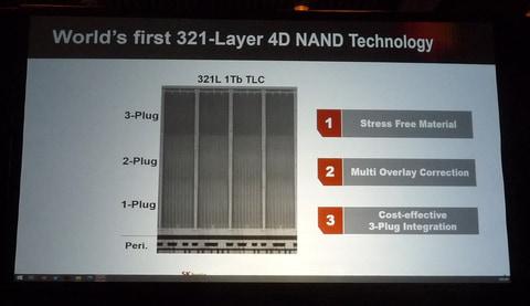
A departure from convention is observed in SK Hynix's approach to stacking layers. Instead of adopting two stacks of 150+ layers each, the company has chosen to implement three stacks, each containing 107 layers. This decision invites comparison with their existing 238-layer product, featuring two stacks of 119 layers. This strategic shift simplifies the manufacturing process of the new NAND package and holds the potential for improved long-term yield rates. Anticipated results project each NAND package delivering a memory density of 20 Gbit per square millimeter or beyond. This figure is nearly twice that of the 176-layer NAND technology in use.
In conclusion, the mentioned advancements highlight the ongoing progress in NAND Flash technology, particularly in terms of program throughput, power efficiency, and manufacturing strategies.
SK hynix's accomplishment of surpassing 300 layers in their 3D NAND flash architecture originates from segmenting the memory cell stack into three parts. This segmentation effectively addresses challenges brought about by increased layer counts, ensuring successful manufacturing. The obstacles posed by elongation and alignment were resolved by selecting low-stress materials and refining alignment techniques.
Additionally, SK hynix's introduction of 5-bit/cell (PLC) technology underscores their commitment to augmenting memory density. This innovative approach divides a memory cell into two sites, enabling the storage of 2.5 bits in each, resulting in a 5-bit data synthesis comparable to the existing TLC method.
SK hynix's roadmap envisions further enhancements in memory density achieved through elevated layer counts and values. This vision involves augmenting dimensions by stacking peripheral circuits and memory cell arrays, a concept termed "4D."
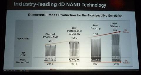
The keynote lecture also unveiled insights into SK hynix's 7th and 8th generation products, highlighting their utilization in gaming consoles and vehicles. The 7th generation, boasting 176 layers, achieved noteworthy monthly mass production volumes, while the 8th generation, featuring 238 layers, initiated mass production of 512 Gbit silicon dies with plans for 1Tbit silicon die mass production. The exhibition showcased the tangible 8th generation 3D NAND flash wafers, exposing their impressive 238-layer design.
SK Hynix Details 321-Layer Ultra-High-Density 3D NAND Flash Technology