Pascal GPU Architecture
The Pascal GPU
The GP104 is based on DX12 compatible architecture called Pascal. Much like in the past designs you will see pre-modelled SMX clusters that hold what is 128 shader processors per cluster. Pascal GPUs are composed of different configurations of Graphics Processing Clusters (GPCs), Streaming Multiprocessors (SMs), and memory controllers. Each SM is paired with a PolyMorph Engine that handles vertex fetch, tessellation, viewport transformation, vertex attribute setup, and perspective correction. The GP104 PolyMorph Engine also includes a new Simultaneous Multi-Projection units. There are 20 active SM clusters for a fully enabled Pascal GP104 GPU. 20 x 128 shader processors makes a total of 2,560 shader processors. Each SM however has a cluster of 64 shader / stream / cuda processors doubled up. Don't let that confuse you, it is 128 shader units per SM. Each GPC ships with a dedicated raster engine and five SMs. Each SM contains 128 CUDA cores, 256 KB of register file capacity, a 96 KB shared memory unit, 48 KB of total L1 cache storage, and eight texture units. The reference (Founders Edition) card will be released with a core clock frequency of 1.61 GHz with a Boost frequency that can run up to 1.73 GHz (and even higher depending on load and thermals). As far as the memory specs of the GP104 GPU are concerned, these boards will feature a 256-bit memory bus connected to a 8 GB of GDDR5 / GDDR5X video buffer memory, AKA VRAM AKA framebuffer AKA graphics memory for the graphics card.
Pascal Graphics Architecture
Let's place the more important data on the GPU into a chart to get an idea and better overview of changes in terms of architecture like shaders, ROPs and where we are at frequencies wise:
 | ||||||
|---|---|---|---|---|---|---|
| Reference GeForce | Titan X | GTX 1080 | GTX 1070 Ti | GTX 1070 | GTX 1060 | GTX 980 Ti |
| 2016 edition | ||||||
| GPU | GP102-400-A1 | GP104-400-A1 | GP104-300-A1 | GP104-200-A1 | GP106-400-A1 | GM200 |
| Architecture | Pascal | Pascal | Pascal | Pascal | Pascal | Maxwell |
| Transistor count | 12 Billion | 7.2 Billion | 7.2 Billion | 7.2 Billion | 4.4 Billion | 8 Billion |
| Fabrication Node | TSMC 16 nm | TSMC 16 nm | TSMC 16 nm | TSMC 16 nm | TSMC 16 nm | TSMC 28 nm |
| CUDA Cores | 3,584 | 2,560 | 2,432 | 1,920 | 1,280 | 2,816 |
| SMMs / SMXs | 28 | 20 | 19 | 15 | 10 | 22 |
| ROPs | 96 | 64 | 64 | 64 | 48 | 96 |
| GPU Clock Core | 1,417 MHz | 1,607 MHz | 1,607 MHz | 1,506 MHz | 1,506 MHz | 1,002 MHz |
| GPU Boost clock | 1,531 MHz | 1,733 MHz | 1,683 MHz | 1,683 MHz | 1,709 MHz | 1,076 MHz |
| Memory Clock | 2500 MHz | 1,250 MHz | 2,000 MHz | 2,000 MHz | 2,000 MHz | 1,753 MHz |
| Memory Size | 12 GB | 8 GB | 8 GB | 8 GB | 3 GB / 6 GB | 6 GB |
| Memory Bus | 384-bit | 256-bit | 256-bit | 256-bit | 192-bit | 384-bit |
| Memory Bandwidth | 480 GB/s | 320 GB/s | 256 GB/s | 256 GB/s | 192 GB/s | 337 GB/s |
| FP Performance | 11.0 TFLOPS | 9.0 TFLOPS | 8.0 TFLOPS | 6.45 TFLOPS | 4.61 TFLOPS | 6.4 TFLOPS |
| GPU Thermal Threshold | 94 Degrees C | 94 Degrees C | 94 Degrees C | 94 Degrees C | 94 Degrees C | 91 Degrees C |
| TDP | 250 Watts | 180 Watts | 180 Watts | 150 Watts | 120 Watts | 250 Watts |
| Launch MSRP ref | $1199 | $499 | $449 | $379 | $249 | $699 |
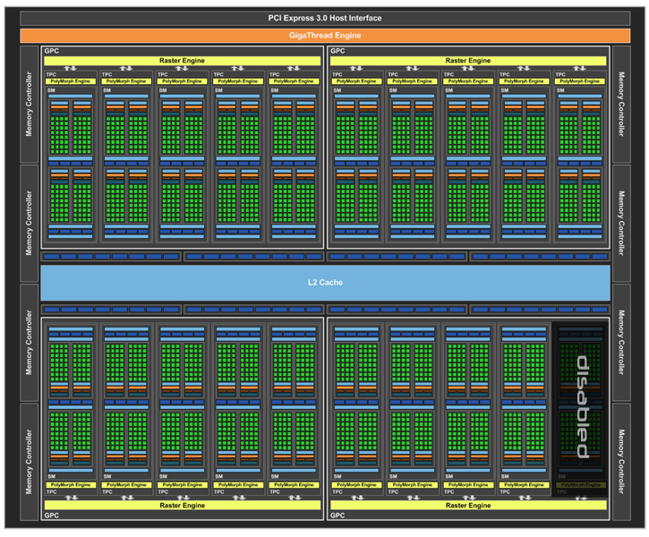
So we talked about the core clocks, specifications and memory partitions. However, to be able to better understand a graphics processor you simply need to break it down into tiny pieces. Let's first look at the raw data that most of you can understand and grasp. This bit will be about the architecture. NVIDIA’s “Pascal” GPU architecture implements a number of architectural enhancements designed to extract even more performance and more power efficiency per watt consumed. Above, in the chart photo, we see the GP104 block diagram that visualizes the architecture, Nvidia started developing the Pascal architecture around 2013/2014 already. Each of the GPCs has 10 SMX/SMM (streaming multi-processors) clusters in total. You'll spot eight 32-bit memory interfaces, bringing in a 256-bit path to the graphics GDDR5 or GDDR5X memory. Tied to each 32-bit memory controller are eight ROP units and 256 KB of L2 cache. The full GP104 chip used in GTX 1080 ships with a total of 64 ROPs and 2,048 KB of L2 cache.
A fully enabled GP104 GPU will have (GTX 1080):
- 2,560 CUDA/Shader/Stream processors
- There are 128 CUDA cores (shader processors) per cluster (SM)
- 7.2 Billion Transistors (FinFet at 16 nm)
- 160 Texture units
- 64 ROP units
- 2 MB L2 cache
- 256-bit GDDR5X
A partially disabled GP104 GPU will have (GTX 1070 Ti):
- 2,432 CUDA/Shader/Stream processors
- There are 128 CUDA cores (shader processors) per cluster (SM)
- 7.2 Billion Transistors (FinFet at 16 nm)
- 152 Texture units
- 64 ROP units
- 2 MB L2 cache
- 256-bit GDDR5
A partially disabled GP104 GPU will have (GTX 1070):
- 1,920 CUDA/Shader/Stream processors
- There are 128 CUDA cores (shader processors) per cluster (SM)
- 7.2 Billion Transistors (FinFet at 16 nm)
- 120 Texture units
- 64 ROP units
- 2 MB L2 cache
- 256-bit GDDR5
What about double-precision? It's dumbed down to not interfere with Quadro sales -- double-precision instruction throughput is 1/32 the rate of single-precision instruction throughput. An important thing to focus on is the SM (block of shader processors) clusters (SMX), which have 128 shader processors. One SMX holds 128 single‐precision shader cores, double‐precision units, special function units (SFU), and load/store units. So based on a full 20 SM (2,560 shader proc) core chip the looks are fairly familiar in design. In the pipeline we run into the ROP (Raster Operation) engine and the GP104 has 64 engines for features like pixel blending and AA. The GPU has 64 KB of L1 cache for each SMX plus a special 48 KB texture unit memory that can be utilized as a read-only cache. The GPU’s texture units are a valuable resource for compute programs with a need to sample or filter image data. The texture throughput then, each SMX unit contains 8 texture filtering units.
- GeForce GTX 960 has 8 SMX x 8 Texture units = 64
- GeForce GTX 970 has 13 SMX x 8 Texture units = 104
- GeForce GTX 980 has 16 SMX x 8 Texture units = 128
- GeForce GTX Titan X has 24 SMX x 8 Texture units = 192
- GeForce GTX 1070 has 15 SMX x 8 Texture units = 120
- GeForce GTX 1070 Ti has 19 SMX x 8 Texture units = 152
- GeForce GTX 1080 has 20 SMX x 8 Texture units = 160
So there's a total of up-to 20 SMX x 8 TU = 160 texture filtering units available for the silicon itself (if all SMXes are enabled for the SKU).
