Graphics architecture
Technology and Specs
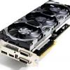
So then, it's time to talk business. The GeForce GTX 680 GeForce GTX 770 being reviewed today is based on Kepler GPU architecture, which we all are familiar with by now. The GeForce GTX 770 is based on the 28nm GK104 GPU, the same as the GTX 680 uses. The 10" long GeForce GTX 770 boasts a good 1536 CUDA (shader processors) cores. The product is obviously PCI-Express 3.0 ready and has a TDP of give or take a typical draw of 170W. But let me first show you the actual GK104 die:
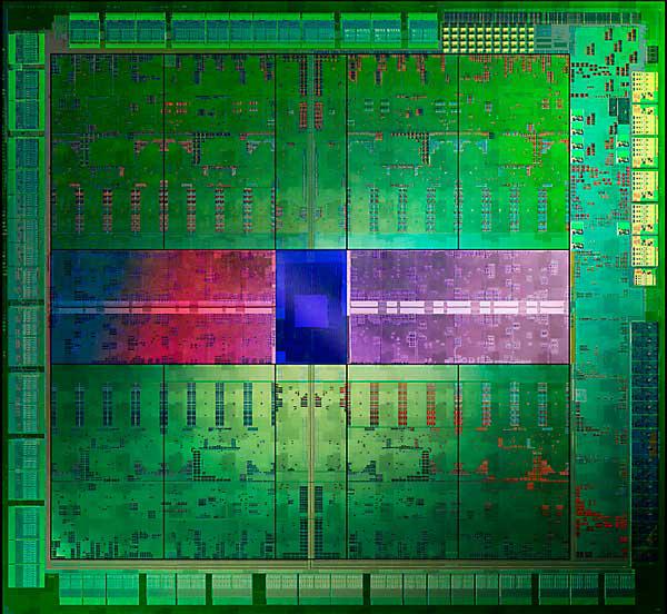
NVIDIA GK104 Kepler architecture GPU used in the Geforce GTX 770
As far as the memory specs of the GK104 Kepler GPU are concerned, the boards will feature a 256-bit memory bus connected to 2 GB or alternatively 4 GB of GDDR5 video buffer memory. On the memory controller side of things you'll see very significant improvements as the reference memory clock is now set at 7 GHz / Gbps. This boils down to a memory bandwidth of 224 GB/s on that 256-bit memory bus. Both the GPU core and the shader processor domain are clocked at 1:1, meaning both the core and shader domain clock in at a 1046 MHz base clock. With this release, NVIDIA now has the first series 700 cards on its way. The new graphics adapters are of course DirectX 11.1 ready. With Windows 8, 7 and Vista also being DX11.1 ready all we need are some games to take advantage of DirectCompute, multi-threading, hardware tessellation and the latest shader 5.0 extensions. For Kepler, NVIDIA kept their memory controllers GDDR5 compatible. Memory wise NVIDIA has nice large memory volumes due to their architecture, we pass 2 GB as standard these days.
The graphics architecture that is Kepler
As you can understand, the massive memory partitions, bus-width and combination of GDDR5 memory (quad data rate) allow the GPU to work with a very high framebuffer bandwidth (effective). Let's again put most of the data in a chart to get an idea and better overview of changes:
| Graphics card | GeForce GTX 480 |
GeForce GTX 580 |
GeForce GTX 680 |
GeForce GTX 770 |
GeForce GTX 780 |
GeForce GTX Titan |
| Fabrication node | 40nm | 40nm | 28nm | 28nm | 28nm | 28nm |
| Shader processors | 480 | 512 | 1536 | 1536 | 2304 | 2688 |
| Streaming Multiprocessors (SMX) | 15 | 16 | 8 | 8 | 12 | 14 |
| Texture Units | 60 | 64 | 128 | 128 | 192 | 224 |
| ROP units | 48 | 48 | 32 | 32 | 48 | 48 |
| Graphics Clock (Core) | 700 MHz | 772 MHz | 1006/1058 MHz | 1046/1085 MHz | 863/900 MHz | 836/876 MHz |
| Shader Processor Clock | 1401 MHz | 1544 MHz | 1006/1058 MHz | 1046/1085 MHz | 863/900 MHz | 836/876 MHz |
| Memory Clock / Data rate | 924 MHz / 3696 MHz | 1000 MHz / 4000 MHz | 1502 MHz / 6008 MHz | 1750 MHz / 7000 MHz | 1502 MHz / 6008 MHz | 1502 MHz / 6008 MHz |
| Graphics memory | 1536 MB | 1536 MB | 2048 MB | 2048 MB | 3072 MB | 6144 MB |
| Memory interface | 384-bit | 384-bit | 256-bit | 256-bit | 384-bit | 384-bit |
| Memory bandwidth | 177 GB/s | 192 GB/s | 192 GB/s | 224 GB/s | 288 GB/s | 288 GB/s |
| Power connectors | 1x6-pin PEG, 1x8-pin PEG | 1x6-pin PEG, 1x8-pin PEG | 2x6-pin PEG | 1x6-pin PEG, 1x8-pin PEG | 1x6-pin PEG, 1x8-pin PEG | 1x6-pin PEG, 1x8-pin PEG |
| Max board power (TDP) | 250 Watts | 244 Watts | 170 Watts | 230 Watts | 250 Watts | 250 Watts |
| Recommended Power supply | 600 Watts | 600 Watts | 550 Watts | 600 Watts | 600 Watts | 600 Watts |
| GPU Thermal Threshold | 105 degrees C | 97 degrees C | 98 degrees C | 95 degrees C | 95 degrees C | 95 degrees C |
So we talked about the core clocks, specifications and memory partitions. Obviously there's a lot more to talk through. To understand a graphics processor you simply need to break it down into smaller pieces to better understand it. Let's first look at the raw data that most of you can understand and grasp. This bit will be about the Kepler architecture, if you're not interested in g33k talk by all means please browse to the next page.
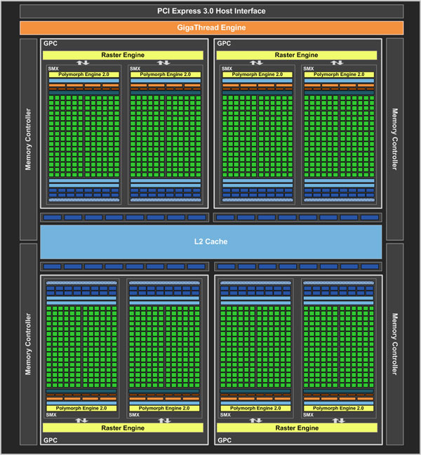
So above we see the GK104 block diagram that entails the Kepler architecture. Let's break it down into bits and pieces. The GK104 will have:
- 1536 CUDA processors (Shader cores)
- 192 CUDA core clusters (SM/SMX).
- 8 geometry units
- 4 raster Units
- 128 Texture Units
- 32 ROP engines
- 256-bit GDDR5 memory bus
- DirectX 11.1
The more important thing to focus on are the SM (block of shader processors) clusters (or SMX as NVIDIA likes to call it for the GTX 680/770, which has 192 Shader processors. That's radically different from Fermi, the GeForce GTX 580 for example had 32 shader processors per SM cluster. 1536 : 192 = 8 Shader clusters (SMs). Let's blow up one such cluster:
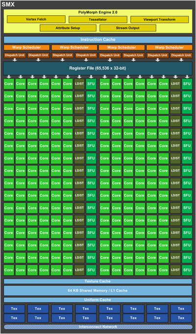
Above the block diagram for a single Shader processor cluster, aka SM or SMX as NVIDIA now calls it. The new SMX has quite a bit more bite in terms of shader, texture and geometry processing. 192 CUDA cores, that's six times the number of cores per SM opposed to Fermi. Now, at the end of the pipeline we run into the ROP (Raster Operation) engine and the GTX 680 again has 32 engines for features like pixel blending and AA. There's a total of 128 texture filtering units available for the GeForce GTX 680. The math is simple here, each SM has 16 texture units tied to it.
- GeForce GTX 580 has 16 SMs X 4 Texture units = 64
- GeForce GTX 680 & 770 have 8 SMs X 16 Texture units = 128
Above the GK104 host interface - The Gigathread engine, four GPCs, four memory controllers, the ROP partitions, a 768 KB L2 cache. Each GPC has eight polymorph engines - ROP partitions are nearby to the L2 cache, each shader cluster is then tied to L1 and a shared L2 cache. Shading performance is going be increased quite bit, geometry performance will get a nice boost as well. NVIDIA is using 64KB Shared Memory/L1 per SMX please note that they have a 16/48 48/16 ratio here for graphics/compute, as before with Fermi. For L2, 128KB per 64-bit memory controller. So that adds up to 512KB L2. In regards to architectural changes, on top of the pipeline NVIDIA has now added new Polymorph 2.0 (world space processing) engines and raster (screen space processing) engines; they act like a mini CPU really.
