Product Teardown
Teardown
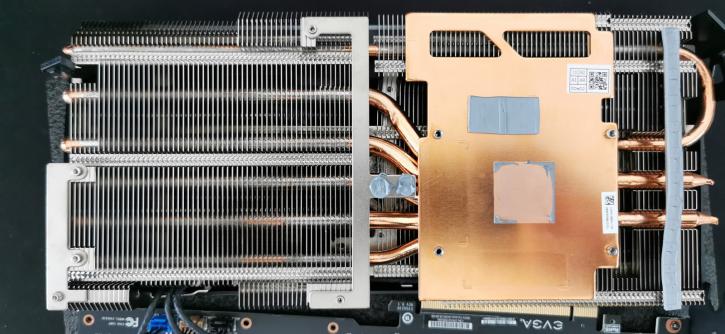
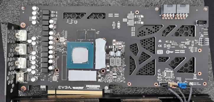
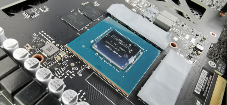
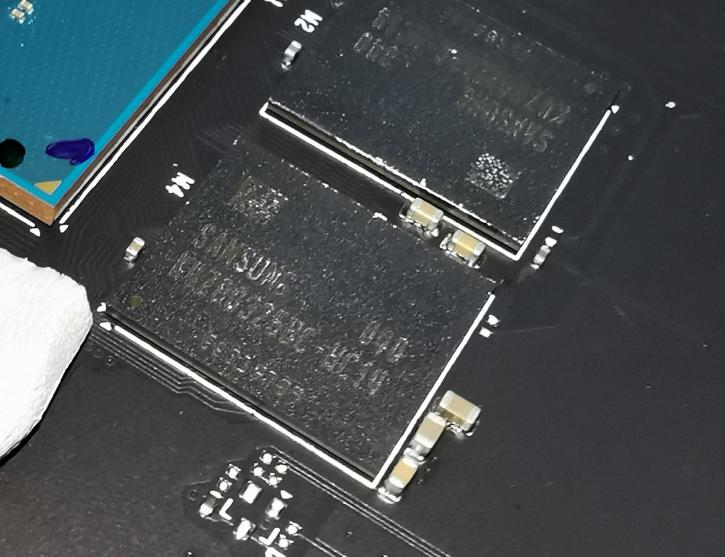
It is a request that is getting more and more daunting as we do not want to damage products. But user request on this is obvious, you guys like a teardown and want to look to see what is going on at the PCB level. So here we go, meet the GA104-300 GPU, GPU and memory power phases, and GDDR6 memory from Samsung (K4Z80325BC-HC14) specced at 1750 MHz (14 Gbps GDDR6 effective). The TIM used was pre-applied as a square patch on the copper GPU block, it however was completely hard and dried out; it still seems to work fine though as temperatures are exellent.
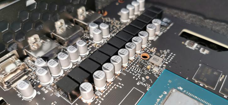
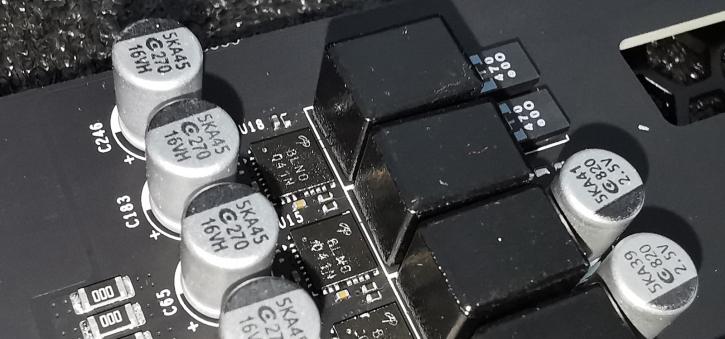
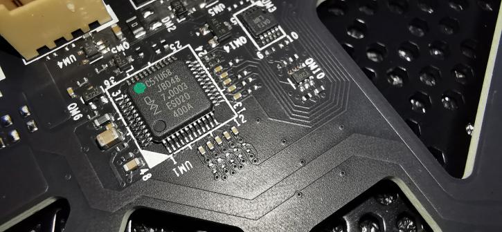
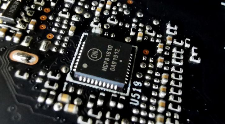
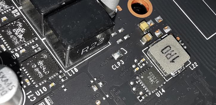
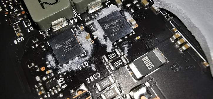
Looking at the PCB, it shows a semi-clean and PCB/component design. Of course, the board does need to be hooked up towards 2x 8-pin PEG connectors. Detected is an OnSemi NCP81610 voltage controller, responsible for 12 phases to the GPU coupled by OnSemi NCP302150 DrMOS. Two phases go to the memory subsystem based on an OnSemi NCP81278T. All components are nicely cushioned with padding and heatsinks, most of them leading to the cooler. The backplane is metal, not plastic, and thus helps a bit with cooling.