Ryzen processor family
The ZEN4 CPU
Zen 4 CPU core-based products will power Ryzen 7000 desktop CPUs (codenamed "Raphael"), high-end mobile processors (codenamed "Dragon Range"), thin & light mobile processors (codenamed "Phoenix"), and Epyc 7004 server processors (codenamed "Genoa" and "Bergamo"). A lot has been said and spoken about ZEN4; AMD single and multi-threaded performance has been excellent overall, but with competition from Intel heating up, they have a new design with lots more cache and turbo frequencies moving to over 5.5 GHz. Overall, Intel was king in High turbo clock frequencies but a notch weaker in IPC. On the other hand, AMD has been very strong on IPC but less so in absolute peak clock frequencies.
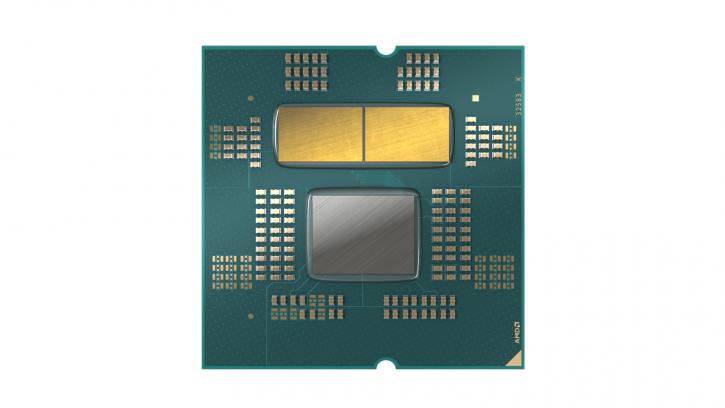
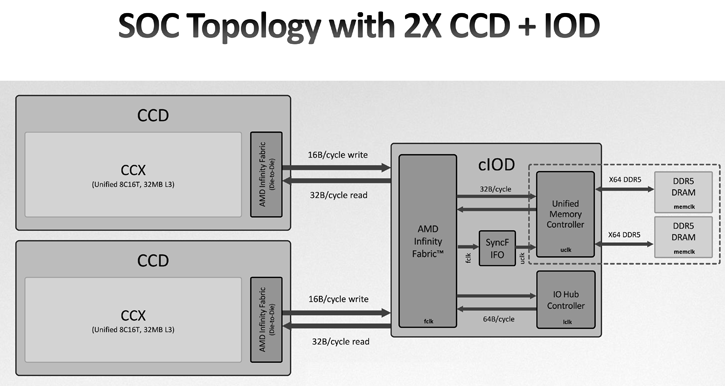
That gave intel advantage in many games with enthusiast performance graphics cards. In the past, a solution to bypass any performance degradation in gaming is to eliminate inter-core and inter-CCX latencies. Initially, ZEN2 addressed that to some extent, with a few efficiency solutions found at cache levels. However, getting rid of the inter-core complex partition latencies is another thing. Zen 4 will continue to use an MCM (multi-chip module), or chiplet design; it will use up to two 8-core CCDs and one I/O die. There will only be one CCX per CCD, and this CCX will consist of eight cores. The Zen 4 core's key architectural advancements include higher data TLBs for the L1 and L2 caches and a doubling of the size of L2 cache per core, from 512KB to 1MB. A translation look-aside buffer (TLB) is a memory cache that stores the most recent virtual memory to physical memory translations. It is used to speed up access to a user's memory location.
| Model | Cores/Threads | Base clock | Boost clock | Cache (L2+L3) | TDP |
| Ryzen 9 7950X | 16C/32T | 4.5GHz | 5.7GHz | 80MB (16+64) | 170W |
| Ryzen 9 7900X | 12C/24T | 4.7GHz | 5.6GHz | 76MB (12+64) | 170W |
| Ryzen 7 7700X | 8C/16T | 4.5GHz | 5.4GHz | 40MB (8+32) | 105W |
| Ryzen 5 7600X | 6C/12T | 4.7GHz | 5.3GHz | 38MB (6+32) | 105W |
So, factors like IPC, Clock frequency, and increased cache sizes will most likely result in performance improvements. In addition, AMD is bringing AVX512 instructions to Zen 4. As a result, applications that exploit this will obtain significantly bigger speed benefits.
Key changes from Zen 3
- AVX-512 instructions support
- L1 and L2 DTLB size increased from 64 to 72 and 2,048 to 3,072 entries
- L2 cache doubled from 512 KiB to 1 MiB per core
- Improved cache load, write and prefetch from/to register (less latency).
- Higher Transistor Density, due to 5nm process
- Capable of higher all-core clockspeeds (shown by AMD to reach 5GHz+ on all cores)
- An igpu in every processor
- PCIe Gen 5.0
- DDR5
There is a total of 64MB of L3 cache (ZEN3 32 MB and ZEN2 had 16MB per CCX ) shared across the cores in the CCX. There's also 1MB of L2 cache per core within the CCX, for 8MB of L2 cache per CCD. Like its predecessor, Zen 4 includes up to two Core Complex Dies (CCDs) manufactured using TSMC's 5nm technology and one I/O die manufactured with 6nm. Previously, the I/O die on Zen 3 was manufactured using GlobalFoundries' 14nm technology. For the first time in any Zen architecture, the I/O die of Zen 4 incorporates RDNA 2 graphics. Zen 4 is the first desktop CPU to utilize the 5nm manufacturing technology. On Zen 4, the L2 cache increased from 512KB to 1MB per core.
Integrated graphics
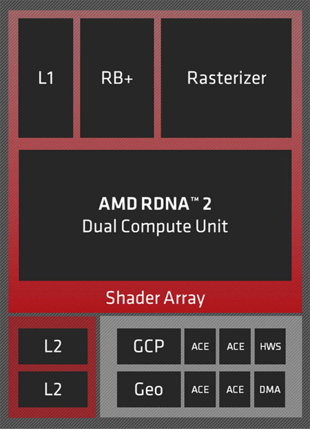
In the past AMD offers CPU and APU's, APUs are a processor with integrated graphics. AMD is seemingly changing this approach as all Raphael Zen4-based processors will be fitted with an RDNA2 graphics unit, which is good news. Those who don't play games or need a separate video card for some other reason needed to purchase a (hopefully) inexpensive card in addition to a standard Ryzen processor or even connect a monitor. This disadvantage grew much more severe due to the scarcity of graphics cards. Every Ryzen 7000 series CPU includes an integrated graphics processing unit, and that IGP resides in the I/O chip (6nm). Even though it is based on the contemporary RDNA2 architecture, it will likely have just two compute units. Therefore, it will not be suited for playing modern games.
Overall, AMD intended to use the smaller 6nm node size to incorporate a nice quality-of-life boost with the addition of graphics capabilities.
Architectural Basics
- 2x RDNA 2 compute units
- 4x ACE
- 1x HWS
- Encode: H.265 10bpc/8bpc, H.264 10bpc/8bpc
- Decode: AV1 10bpc/8bpc, VP9 10bpc/8bpc, H.265 10bpc/8bpc, H.264 10bpc/8bpc
- Display:
- HDMI 2.1 with: HFR, 48Gbps FRL, DSC, HDR10+, and VRR extensions
- DisplayPort 2.0 Ready with: Adaptive-Sync, DSC, UHBR10, and HDR extensions
