
Article - Guide - Review
An introduction to High Bandwidth Memory
AMD has been teasing about its next-gen Radeon (R9 390X we assume) graphics cards and processors back in early May. It is without doubt that at least some of the upcoming graphics cards will be the first to feature high-bandwidth memory (HBM), let's call is the turbo-charged offspring to GDDR5 memory, used in today’s graphics cards.
AMD briefed press on HBA last week - High Bandwidth Memory, something they started working on roughly seven years ago. This new type of graphics memory is going to change the para-dime in the graphics industry when we are talking about using less power, smaller form factors but most of all increased & scalable memory bandwidth. In this article we'll dig a little deeper into the new technology.
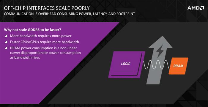
We've talked about and mentioned HBM many times in the front-page news already. HBM is short for High Bandwidth Memory, basically a new technology that was invented and brainstormed many years ago. With fabrication technology shrinking the time was right for AMD to move forward with their first implementation of HBM. HBM v1 will be introduced soon in products that can not be discussed just yet. There are several advantages to HBM memory, but of course also some concerns. First and foremost, the memory bandwidth that this technology can potentially offer is colossal. But why the move to HBM?
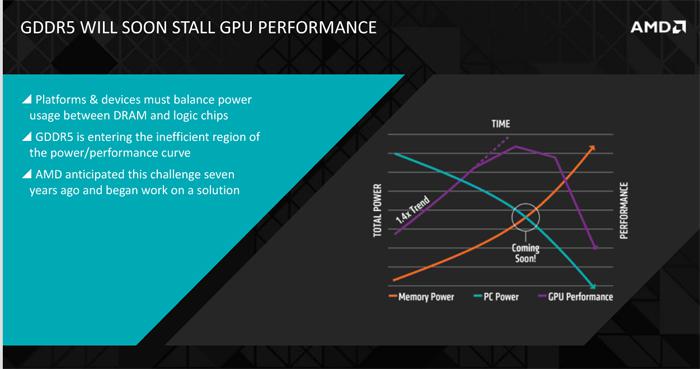
AMD and other manufacturers have been facing the issue that GDDR5 memory is slowly becoming rather inefficient when it comes to power used versus performance delivered. More chips, more density more voltage. HBM offers a three-fold improvement in performance per watt compared to GDDR5, and a 50-percent increase in power savings, according to AMD.
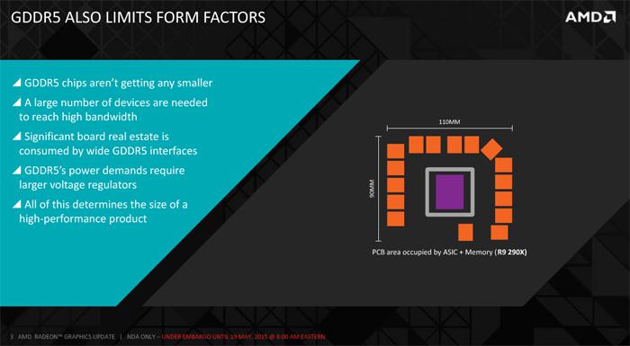
So while GDDR5 is capable, the past few years GDDR5 has become faster, DRAM volume sizes have increased, more ICs in number are used and the DDR packages have become bigger, these things all require more power and and along with it larger voltage regulators higher latency and what not. With HBA memory on-die rather than on-card, it can be used for a lot of really interesting form factors as it will use less power, that in turn can be used for other stuff like the GPU.
On-die e.g. on-chip, that will be something to get used to. The approach is going to vastly different as the memory will no be placed next to the GPU on the actual silicon die. So the notion of DDR memory ICs spread out over the PCB are a thing of the past with HBA. That means smaller PCBs, and with the graphics memory so close to the GPU, shorter, wires less latency and less efficiency issues as well. Being so close to the GPU/APU/SoC is efficient, and the companies are not tied to incredible complex designs, wires can be used in a multitude and as such you'll see a move from say a 256-bit wide memory bus towards a 1024-bit wide memory bus with High Bandwidth Memory (per package).
We'll discuss AMDs HBM implementation a little more in detail on the next page.
