An Architecture Change
Right, before we dive into the photo-shoot and benchmarks, first we are going to walk trough the architecture that is Cayman, the GPU embedded on the Radeon HD 6950 and 6970.
An Architecture Change
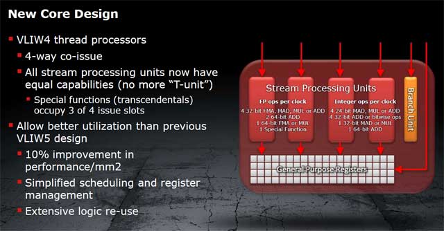
The previous released cards in the 6800 Barts series, the 6850 and 6870, were merely a small architectural optimization/tweak over the last generation Cypress architecture. With the Cayman GPU, things have changed a little bit as the fundamental section of the GPU, the Shader processor setup underwent a significant change, and we are still debating whether or not it was a good one.
AMD moved from a VLIW5 (also knows as VEC5) towards a VLIW4 SIMD shader processors setup. We are not going to discuss the VLIW4 thread processor setup in much detail but basically what this means is that AMD went from a VLIW5 configuration, that used four simple SIMD units and one complex t-unit (transcendental unit) in order to build a stream processing unit, to a VLIW4 configuration that uses four stream units which feature equal capabilities, two of them being assigned with special functions.
AMD however claims this change will bring them 10% more performance over the previous thread processor setup, better scheduling and register management. We think it was merely a design change to save on the number of transistors which you can re-use to add more shader processors on the processor die.
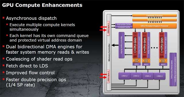
Next to this rather significant change there are more changes to be found on the graphics card. It has upgraded render back ends (ROPS) with a redesigned Z-Stencil and ROP unit architecture consisting of 128 Z/Stencil ROPs, and 32 color ROPs, up to 2 times faster in 16-bit integer operations and two to four times faster in 32-bit floating point operations which you will have in AA performance, much faster GDDR5 memory and we also spot a series of improved compute features that will help out in the performance in that segment.
One other detail that you might find interesting is that when you look at the block diagram, you'll notice that the GPU pretty much looks like a dual-core processor. AMD calls this dual graphics engines. Anyway, have a peek at the block diagrams if at all interested.
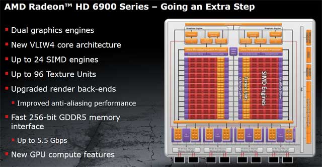
Alright, some more generic information to grasp. The Cayman GPU itself is based on a 40nm fabrication process and harbors a blistering 2.64 Billion transistors. The graphics engine can have up-to 24 shader clusters, with each engine holding 64 shader processors. Do the reverse math and you'll quickly learn that the most high-end GPU will count 1536 shader processors. A bit of an unusual number and we just wonder if there isn't more of them to be found inside that die really.
The Cayman chip has up-to 96 Texture Units and can produce 2.7 TFLOPs of single precision performance.
Memory wise AMD of course stuck to it's fine working GDDR5 setup, and yes... it is still based on a 256-bit memory bus. They did increase the effective data rate though, the fastest product today will run a 5500 MHz (effective) memory clock frequency. We continuously say "effective" as GDDR5 memory is quad data rate memory. So 5500 MHz in fact is 4x 1375 MHz.
Very notable is that these cards all come with 2 GB of memory, that's both the R6950 and R6970. But lets look into the specifications a little more in-depth, next page please.
Specifications
So then, based on Cayman, initially two products are thus released, the Radeon HD 6950 and 6970. At a later stage in time we expect the product under codename "Antilles" to have two Caymen GPUs for what we all know as a dual-GPU graphics card. Here are the particulars for the two products released today placed into a table.
| Radeon HD 6950 | Radeon 6970 | |
| Fab Process | 40nm | 40nm |
| Die Size | 389 mm2 | 389 mm2 |
| Transistors | 2.64 Billion | 2.64 Billion |
| Core Clock / MHz | 800 | 880 |
| Memory Clock / MHz | 5000 | 5500 |
| Memory Bandwith | 160 GBps | 176 GBPs |
| Memory type | GDDR5 | GDDR5 |
| Shader processors | 1408 | 1536 |
| Compute performance | 2.25 TFLOPS | 2.7 TFLOPS |
| Color ROPs | 32 | 32 |
| z/Stencil ROPs | 128 | 128 |
| TDP | 140 W | 190 W |
| Idle power | 20 W | 20 W |
The Radeon HD 6950 comes armed with 1408 Shader processors, thus 22 SIMD based shader clusters, split up in a twofold engine. The domain and shader clock is locked in at 800 MHz. The card comes paired with 2 GB of memory clocked at (effective) 5000 MHz. The TDP of this product is 140 W which can be extended to 200 W board power with a new feature called PowerTune which we'll explain later.
Let's have a quick comparative overview of some of the specifications representing a certain scope of other performance parts:
| Specifications | Radeon HD 5850 | Radeon HD 6850 | Radeon HD 6870 | Radeon HD 6950 | MSI R6950 TFIII OC |
Radeon HD 6970 |
| GPU | Cypress Pro | Barts Pro | Barts XT | Cayman Pro | Cayman Pro | Cayman XT |
| Manufact. tech. | 40 nm | 40nm | 40nm | 40nm | 40nm | 40nm |
| GPU frequency | 725 MHz | 775 MHz | 900 MHz | 800 MHz | 850 MHz | 880 MHz |
| Stream processors | 1440 | 960 | 1120 | 1408 | 1408 | 1536 |
| Memory Datarate | 4000 MHz | 4000 MHz | 4200 MHz | 5000 MHz | 5200 MHz | 5500 MHz |
| Memory bus | 256-bit | 256-bit | 256-bit | 256-bit | 256-bit | 256-bit |
| Memory buffer |
1 GB GDDR5 | 1 GB GDDR5 | 1 GB GDDR5 | 2 GB GDDR5 | 2 GB GDDR5 | 2 GB GDDR5 |
| Power consumption |
151 W | 127 W | 150 W | 150 W | 153 W | 190 W |
| Idle Power |
- | 19 W | 19 W | 20 W | 20 W | 20 W |
Both cards are of course up-to-date DX11 class product with a couple of new features. Features wise, both graphics cards will be very similar to the last generation products and is merely an advanced, updated model. However some features like DisplayPort now follows 1.2 interface specification, HD3D, UVD3 and HDMI 1.4a are introduced. We also spot a new Anti-aliasing mode (Morphological AA), better Anisotropic filtering and improved Tessellation performance up-to twice the performance of that of the 5000 series.