So what's the SE all about in the GF104 GPU
So what's the SE all about in the GF104 GPU
So then, the GeForce GTX 460 SE. We are first going to discuss REFERENCE specifications, clocks and features.
Typically, we dive deeply into the graphics core architecture. For this article, I would like to keep things a little bit more simple and easy to grasp -- to keep things understandable.
The GeForce GTX 460 SE series is to be based on the ~2 Billion transistors encounting GF104 chip.
It is the very same chip used on the regular GTX 460 cards. A less complicated chip to manufacture as the smaller transistor count directly relates to better yields, better heat levels, better voltages and thus a better TDP as well. It is a smaller chip to produce.
Currently NVIDIA puts the GF104 chip onto three products, the GeForce GTX 460 with 768MB of graphics memory, the GeForce GTX 460 with 1024MB of memory and now the SE edition with 1024MB of memory.
For the bigger part of the specifications, the two older cards are similar when it comes to shader processor count, memory bus and clock frequencies, the 1GB model however definitely will be a good chunk faster, as cutting away 256MB of memory also cuts away a chunk of the ROP engine.
The SE edition will have another SM (shader processor cluster of 48 shader processors) unit cut away bringing the shader count from 336 processors back to 288 processor. It does get to keep the full ROP count, yet does forfeit a little on clock frequencies. It however gains again in memory size. Very confusing we agree. But let's compare specs a little more in-depth to get a better grasp of what is going on.
Reference specifications:
| Graphics card | GTX 460 SE | GTX 460 768MB | GTX 460 1024MB |
| Graphics Processing Clusters | 2 | 2 | 2 |
| Streaming Multiprocessors | 6 | 7 | 7 |
| Shader processor | 288 | 336 | 336 |
| Texture Units | 48 | 56 | 56 |
| ROPs | 32 | 24 | 32 |
| Core Clock | 650 MHz | 675 MHz | 675 MHz |
| Shader Clock | 1300 MHz | 1350 MHz | 1350 MHz |
| Memory Data rate | 3400 MHz | 3600 MHz | 3600 MHz |
| Graphics Memory | 1024MB GDDR5 | 768MB GDDR5 | 1024MB GDDR5 |
| Memory interface | 256-bit | 192-bit | 256-bit |
| Memory bandwidth | 81.6 GB/s | 86.4 GB/s | 115.2 GB/s |
| Fab node | 40nm | 40nm | 40nm |
| TDP | 150 Watts | 150 Watts | 160 Watts |
So, the card in reference setup will be clocked at 650 MHz on the core frequency, and in NVIDIA's typical 1:2 setup mode 1300 MHz on the now 288 shader processors. There will be a lot of overclocking headroom on these boards as 775 MHz should not be an issue (even without voltage tweaking).
The GDDR5 memory will be clocked at a slightly shy 3.4 Gbps which is 3400MHz effectively (quad data rate). The card will make use of four 64-bit memory controllers which boils down to 256-bit memory for this 1024 GB model.
The cards are based on a dual slot cooling design and come with two dual-link DVI and a mini-HDMI connector. HDMI will again pass sound through, including bit streaming support for Dolby True HD and DTS-HD Master. Being a mid-range product, only 2-way SLI will be allowed and thus you'll only see a single SLI finger/connector on the PCBs. Okay, the next stop will be an extensive photo-shoot.
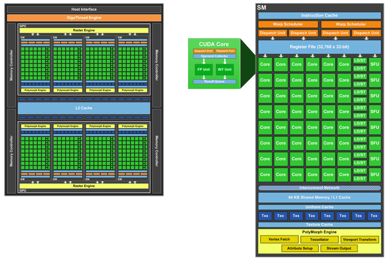 To your left, two out of the eight shader processor clusters will be disabled. Each cluster (SM) has 48 shader processors. Since the GF104 has eight of them, we wonder if in the future we'll see a 384 SP encounting product ?
