α Lyrae
α-Lyrae: VEGA
AMD VEGA architecture preview
Captains log, it is December the 7th, like an eagle I am mid-air, however in-between Europe and the USA while writing this introduction. Listening to Bill Withers and yes, it absolutely will be a lovely day. I am on my way to a jam-packed event where AMD is briefing tech-media not just on ZEN RYZEN processors, but VEGA as well. For those of you that have lived under a rock the past year, when I refer to VEGA I do refer towards the graphics processor that is based on VEGA10 architecture, aka what for the consumer likely is going to be the Radeon RX 490 series graphics cards.
Vega, also designated Alpha Lyrae (α Lyrae, abbreviated Alpha Lyr, α Lyr), is the brightest star in the constellation of Lyra, the fifth-brightest star in the night sky and the second-brightest star in the northern celestial hemisphere, after Arcturus. It is relatively close at only 25 light-years from the Sun, and, together with Arcturus and Sirius, one of the most luminous stars in the Sun's neighborhood. Vega has been extensively studied by astronomers, leading it to be termed “arguably the next most important star in the sky after the Sun. The traditional name Vega (earlier Wega) comes from a loose transliteration of the Arabic word wāqi‘ meaning "falling" or "landing", via the phrase an-nasr al-wāqi‘, "the falling eagle".
A lot has been said and spoken regarding this graphics card series. It probably has been one of AMDs best kept secrets to date. Unfortunately, it is still not here or released. It however indicative is that it will be a bit of a beast and that gives AMD the opportunity to compete with the GeForce GTX 1080 from Nvidia, that much we can share already.
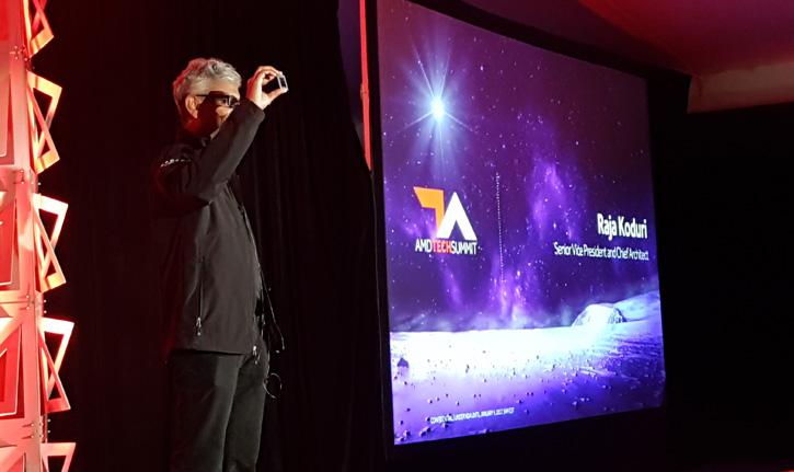
AMD's CTO of the Graphics Product Group, Raja Koduri holding a VEGA GPU
A reality however is that you are not going to see VEGA based graphics cards in the stores anytime soon. AMD made it clear on the media-event that the enterprise market (not the space ship) will be served first. You probably already have read our content on the AMD Radeon Instinct announcement which includes a VEGA GPU powered MI25 Accelerator. Indicative of low yields and volume availability, AMD simply will introduce VEGA where they can make the most money, and for now that will be enterprise solutions. So the first iteration of VEGA will be the Radeon Instinct MI25 with Vega GPU listed at 25 TFLOPS (fp16). VEGA for consumers could be anywhere from 10 to 12.5 TFLOP of single precision (fp32-bit) game performance depending on its final configuration. Considering a reference clocked GeForce GTX 1080 offers 9 TFLOPs and a GTX Titan X (Pascal) is at roughly 11 TFLOPS we can assume that the performance is there. With that said (and this is pure speculation) I honestly do not expect VEGA to launch for consumers in the form of a Radeon RX 490 anytime sooner than Q2 of 2017. Likely in the Computex time-frame, perhaps a bit sooner.
An architecture preview
This is an architecture preview hence we do have a thing or two to share with you today. Let's get the elephant out of the room first and confirm something. Yes, VEGA, (well VEGA10) will be fitted with HBM2 memory as well as a new IO gateway and that cache dubbed High Bandwidth Cache. Vega is a GPU with 200 new features. A handful of things are key for AMD with this very scalable GPU new architecture. Now I deliberately state new architecture here as that much is a fact, VEGA is not based upon Polaris, this is a completely new chip and architecture with a new programmable geometry pipeline as well.
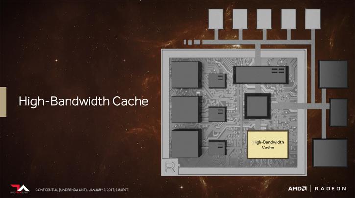
Vega 10 is using High Bandwidth Video Memory, VRAM, graphics memory or whatever you like to call it. The specific type flavor or flavah-flaf used is HBM2 memory. The graphics gawds from AMD claim that HBM2 will offer you 5x the power efficiency compared to any other graphics memory including GDDR5, and yes that is huge. Another benefit obviously is capacity. HBM is on-chip vertically stacked (slabs of memory cells placed on top of each other) and you know it, when it comes to caches and memory bigger is simply better (in terms of storage volume). With the second iteration of HBM, HBM2 AMD now has 8x the density per stack with a 50% smaller footprint. So again, not to confuse anybody, frame-buffer or graphics memory is now referred to as HB (high bandwidth) cache here. I'll let you in on a little secret (AMD has not disclosed this much), but you may can expect 8 GB for the initial VEGA based products.
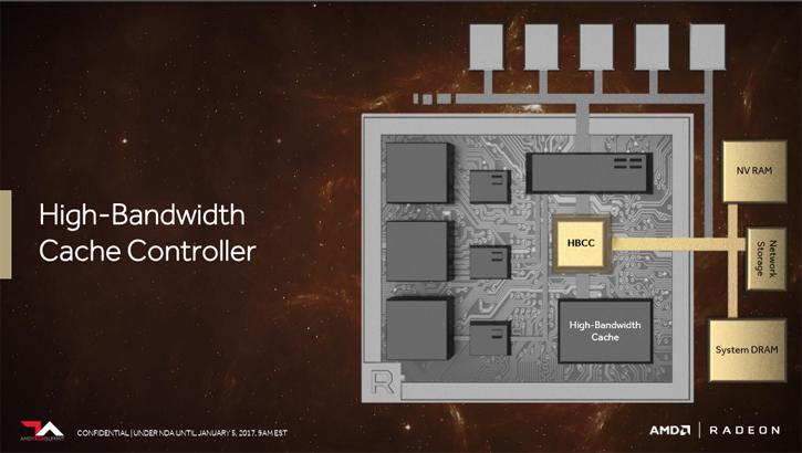
Managing all that lovely stacked memory requires a memory controller, well actually that is plural, controllers. AMD has completely revamped it and added a number of things while they were at it, including it to be an IO gateway. The High Bandwidth Cache Controller as AMD touts it, enables AMD to access 512TB virtual address space (and no I did not misspell that... Terabyte). It enables the GPU to have adaptive, fine grained data movement throughout the chip and whatever it is connected to. The HBCC isn't just managing and accessing pools of HBM memory, it also has a link to NVRAM (Non-volatile random-access memory (NVRAM) is random-access memory that retains its information when power is turned off i.e. non-volatile), as well as your System DRAM aka your system memory aka Dynamic random-access memory (DRAM). DRAM is a type of random-access memory that stores each bit of data in a separate capacitor within an integrated circuit. The capacitor can be either charged or discharged; these two states are taken to represent the two values of a bit, conventionally called 0 and 1.
