Product Showcase
Product Showcase
The following images were taken at high-resolution and then cropped and scaled down. The camera used was a Canon DSLR shooting 24 MegaPixel photos. Right then, off we go.
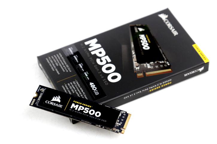
The sample we have at hand is the 480 GB M.2 model. Performance is listed as 3000 MB/s for reads and 2400 MB/sec for writes with roughly 210K IOPS at 4k random writes QD32 aligned disk access with our tested model.
Above, the tested unit; you should easily be able to place the M.2 unit into a compatible motherboard. Most Z97/X99/Z170 and upcoming Z270 motherboards support it. You should however check out with the motherboard manufacturer if you have a x4 lane PCIe version with NVMe support.
The compact M.2 2280 (2280 = 80mm) form factor ensures compatibility with next-generation desktop and mobile platforms that support the M.2 PCIe slot and interface.
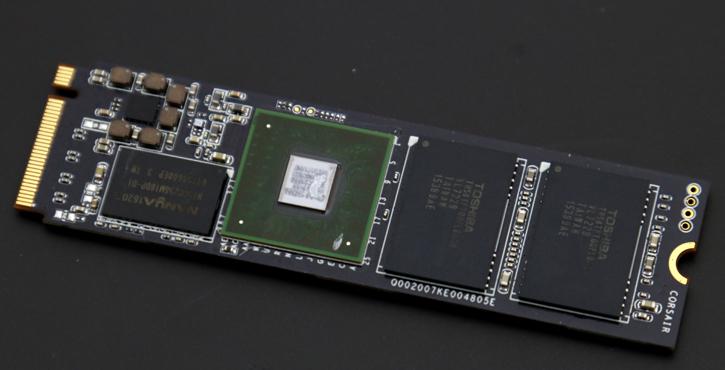
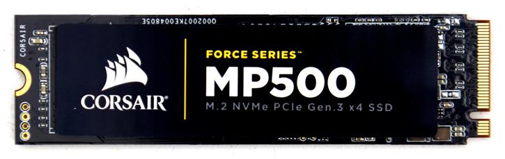
On top of the SSD is a protective sticker glued, this is actually a copper induced sticker and spreads out heat over that sticker. We'll show you that effect with our thermal image camera. For our review obviously we had to remove it to show you da goods under da hood.
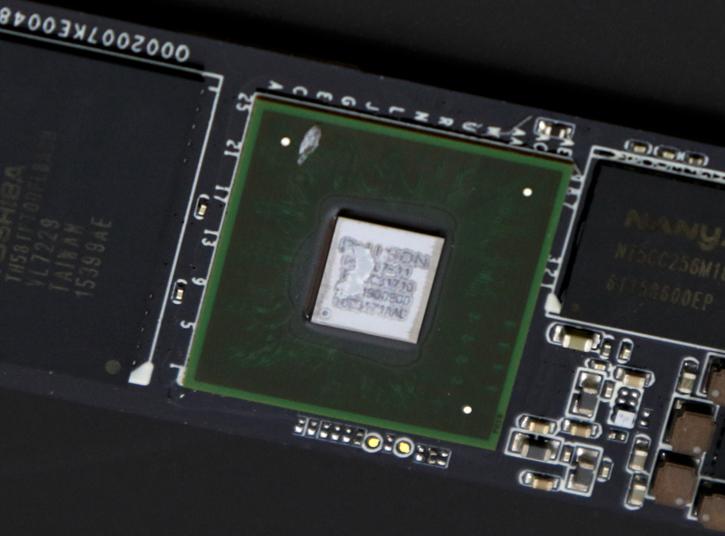
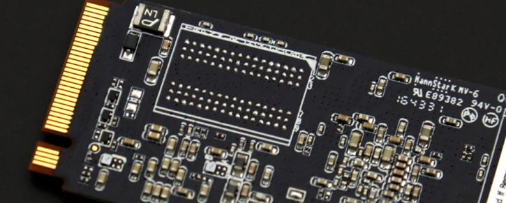
The PCB reveals a Phison PS2007-E7 NVMe controller. The PS5007-E7 supports 1Znm SLC/MLC/TLC as well as the latest 3D (vertically stacked) NAND. These controllers support up to 2 Terabytes today and will expand to 4 Terabytes in the coming future. PS5007-E7 also supports NVMe L1 sub-state with less than 5mW in L1.2 low power mode.
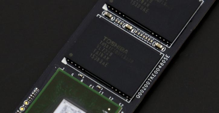
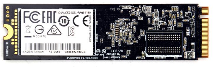
It's a bit washed out but that reads TH58TFT0DFLBA8H. It is a Toshiba 15nm MLC NAND flash memory. You'll find four flash packages, two on each side of the PCB.
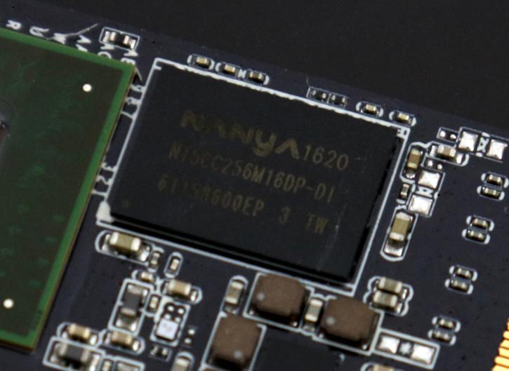
Corsair 480GB configuration uses a 1024MB DRAM buffer that the company deploys in a single package from Nanya.
Perhaps in the future a 1 TB version will be launched as the backside of the PCB reveals an empty SMT trace for another DRAM chip.
