In other news today, one of the most popular cards for NVIDIA right now has to be the GeForce GTX 260. It recently already received the new 55nm GPU (G200b), yet as it seems another update can be expected, to reduce manufacturing costs and further drive down prices.
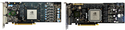
The new PCB design is P654 and we spot several new changes. All memory chips are now located at the GPU side of the PCB. Voltage regulators are also repositioned. News from Expreview suggests that NVIDIA has worked out yet another (newer). PCB reference design model: P897 with one thing in mind, ramp down production costs even more. According to Techpowerup the reference design graphics board based on the PCB will be given the internal name "D10U-20".
- The number of PCB layers has been reduced from 10 to 8, perhaps to compress or remove blank, redundant or rudimentary connections
- A 4+2 phase NVVDD power design using the ADP4100 voltage regulator IC, the FBVDDQ circuit has been reduced from 2 phases to 1, and the MOSFET package has been changed from LFPAK to DPAK grouping, to reduce costs. The ADP4100 lacks the I2C interface, which means voltage control will be much more difficult than on current PCBs of the GeForce 260,280, 285 and 295
- The optional G200b support-brace has been removed
- While the length of the PCB remains the same, the height has been reduced to cut costs
- BIOS EEPROM capacity reduced from 1 Mbit (128 KB) to 512 Kb (64 KB)
- Cheaper DVI connectors