Product PCB and component overview
Product PCB and component overview
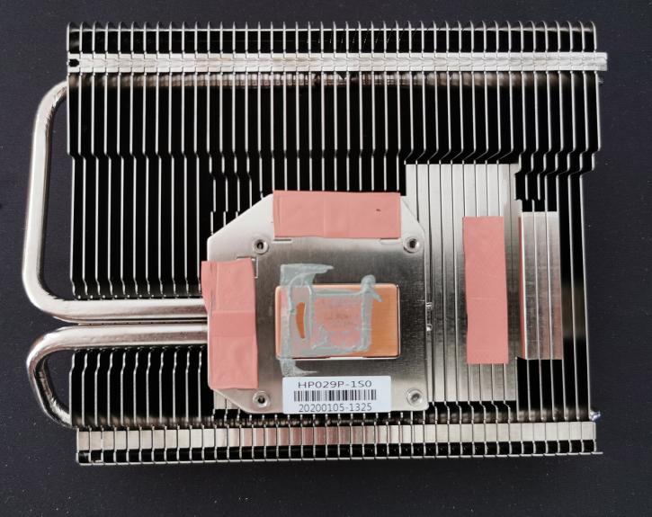
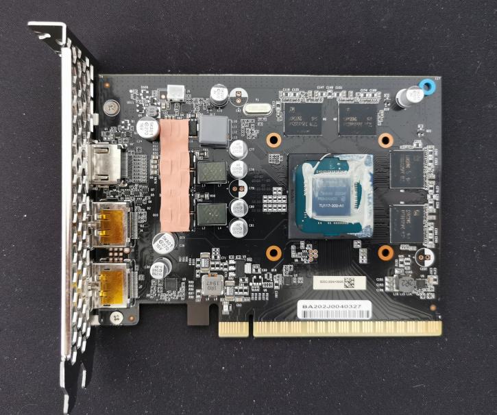
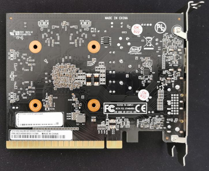
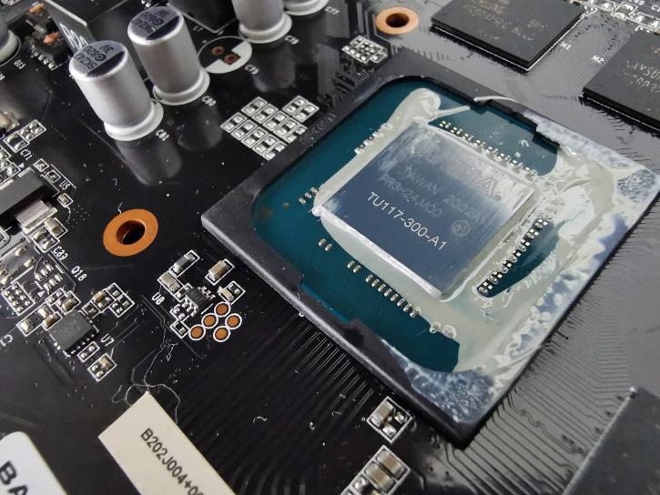
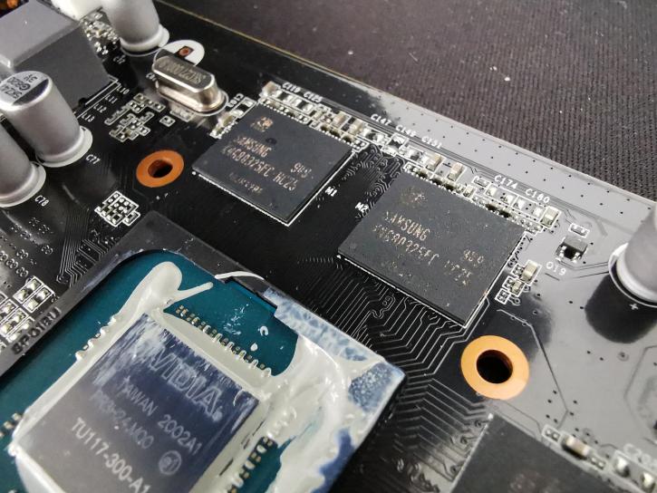
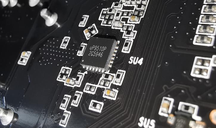
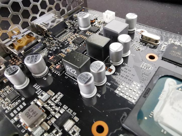
In the photos below you can see a number of things. This card was fitted with GDDR5 memory chips fabbed by Samsung. Photos show the 12nm based TU117-300-A1 GPU fabbed on a 12nm node by TSMC. The chip has a 200 mm² die size with 4.70 billion transistors. Powered by merely a 2 phase power design for the GPU managed by a uP9510P, and then one phase for memory.
- PCB frontside (High-res)