The platform
X670E/X670, and B650E/B650 Motherboards
AMD AM5 infrastructure features new chipsets, including the X670E, X670, B650E, and B650. These chipsets will be part of the 600-series platform that supports DDR5 memory and PCI Express Generation 5. The X670E chipset, in particular, is optimized for extreme performance and can support two video card ports and PCIe Gen 5 M.2 slots for high-speed SSDs. These chipsets will be part of the 600-series platform that boasts DDR5 memory and PCI Express Generation 5 for both storage and graphics. The platform offers a total of 24 PCIe 5.0 lanes, with 16 dedicated to the video card, four for an M.2 slot, and another four for chipset connection. AMD has emphasized that the X670E chipset is designed for unparalleled capability and extreme overclocking, and its PCI Express Gen 5 support is comprehensive.
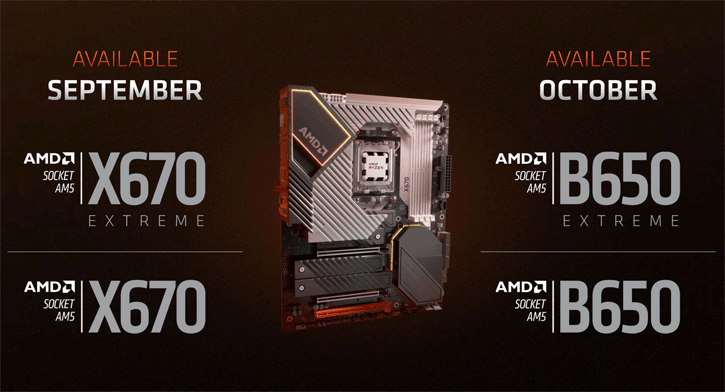
An X670 is designed for Enthusiast Overclocking and features support for Gen5 storage and optional graphics. Only the PCIe Gen5 storage standard will be supported by the mainstream platform based on the B650 chipset. The motherboard part of the 600 series will also include up to 14 SuperSpeed USB 20 Gbps (TypeC), and WiFI-E6 with DBS/Bluetooth Low Energy 5.2. Interestingly. Additionally, AMD has announced that the motherboards in the 600-series will come equipped with up to four HDMI 2.1 and DisplayPort 2 outputs. Mainboards with the chipsets B650 and B650E are expected to push the new socket AM5 platform for Ryzen 7000 CPUs into the lower-priced territory. The X670 and X670E variants are projected to be quite pricey.
The distinctions between the B650(E) and the X670 (E)
The differences between the chipsets are illustrated in this AMD picture. The B650(E) only has half as many USB and SATA ports as the X670 versions. PCIe 5.0 is optional on the B650 and is exclusively meant for an M.2 SSD port. The B650E, on the other hand, has PCIe 5.0 for both the graphics card and an SSD, for a total of up to 20 PCIe 5.0 lanes.
Socket AM5
AM4 has been serving since 2016; AMD's Ryzen 7000 series has announced its retirement of the socket AM4 platform. This marks AMD's transition to PCI Express 5.0 and DDR5 memory. The AM5 LGA socket contains 1718 pins, which significantly increased over the AM4 socket, which had 1331. That increase is partly needed for DDR5, and 24 PCIe 5.0 lanes. Four lanes presumably just link to the chipset. After allocating 16 lanes to the graphics card, there will be 8 lanes left, four for direct-CPU-attached M.2 SSDs and four are used as interconnect. Remember, though, PCIe 5.0 video cards are not yet available. BTW your CPU cooler you can carry over towards the new platform as they will be compatible between AM4 and AM5 with the same mounting system
DDR5
The new platform will officially support DDR5. The controller is officially compatible with speeds up to DDR5-5200 (JEDEC default). However, AMD's Ryzen 7000 Zen 4 CPUs appear to have a sweet spot of DDR5-6000, allowing for a 1:1 IFC ratio (Infinity fabric Interconnect). A 1:1 ratio means that the memory runs at the same frequency as the memory controller on the CPU, which is the best-case scenario. With Alder, Intel has separated the memory ranks into two categories: a 2:1 mode known as Gear 2 that is the DDR5 default, and a 4:1 version known as Gear 4. A 1:1 ratio offers the advantage of allowing for lower latencies and faster speeds. A higher ratio, on the other hand, allows for better overclocking and faster data transfer rates but also results in higher latencies. DDR5-6000 for AMD Ryzen 7000 "Zen 4" CPUs already sounds amazing for AM5, with a default to DDR5-5600. Higher frequency DIMMs are supported; however, if you exceed the DDR5-6000 limit, you will be forced to use a 1:2 IFC. DDR5-6400 operating at 1:2 is said to offer poor results and is not advised if you want better gaming performance. AMD has been working on a new overclocking standard for DDR5 memory called EXPO, which the company intends to use as a competitor to Intel's XMP 3.0 protocol. AMD revealed earlier this year that it is working on Ryzen Accelerated Memory Profiles. EXPO will be the memory modules equivalent to Intel XMP 3.0, storing compatible ddr5 overclocking profiles with faster speeds and tighter frequencies. It is also advertised as a one-click memory overclocking solution.
The ZEN4 CPU
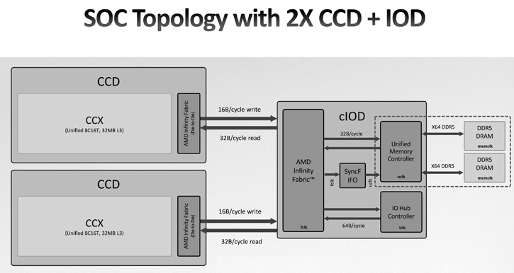
Zen 4 CPU core-based products will power Ryzen 7000 desktop CPUs (codenamed "Raphael"), high-end mobile processors (codenamed "Dragon Range"), thin & light mobile processors (codenamed "Phoenix"), and Epyc 7004 server processors (codenamed "Genoa" and "Bergamo"). A lot has been said and spoken about ZEN4; AMD single and multi-threaded performance has been great overall, but with competition from Intel heating up, they have a new design with lots more cache and turbo frequencies moving to over 5.5 GHz. Overall, Intel was king in High turbo clock frequencies but a notch weaker in IPC. On the other hand, AMD has been very strong on IPC but less so in absolute peak clock frequencies. That gave intel advantage in many games with enthusiast performance graphics cards. In the past, a solution to bypass any performance degradation in gaming is to eliminate inter-core and inter-CCX latencies. Initially, ZEN2 addressed that to some extent, with a few efficiency solutions found at cache levels. However, getting rid of the inter-core complex partition latencies is another thing. Zen 4 will continue to use an MCM (multi-chip module), or chiplet design; it will use up to two 8-core CCDs and one I/O die. There will only be one CCX per CCD, and this CCX will consist of eight cores. The Zen 4 core's key architectural advancements include higher data TLBs for the L1 and L2 caches and a doubling of the size of L2 cache per core, from 512KB to 1MB. A translation look-aside buffer (TLB) is a memory cache that stores the most recent virtual memory to physical memory translations. It is used to speed up access to a user's memory location. So, factors like IPC, Clock frequency, and increased cache sizes will most likely result in performance improvements. In addition, AMD is bringing AVX512 instructions to Zen 4. As a result, applications that exploit this will obtain significantly bigger speed benefits.
Key changes from Zen 3
- AVX-512 instructions support
- L1 and L2 DTLB size increased from 64 to 72 and 2,048 to 3,072 entries
- L2 cache doubled from 512 KiB to 1 MiB per core
- Improved cache load, write and prefetch from/to register (less latency).
- Higher Transistor Density, due to 5nm process
- Capable of higher all-core clockspeeds (shown by AMD to reach 5GHz+ on all cores)
- An igpu in every processor
- PCIe Gen 5.0
- DDR5
There is a total of 64MB of L3 cache (ZEN3 32 MB and ZEN2 had 16MB per CCX ) shared across the cores in the CCX. There's also 1MB of L2 cache per core within the CCX, for 8MB of L2 cache per CCD. Like its predecessor, Zen 4 includes up to two Core Complex Dies (CCDs) manufactured using TSMC's 5nm technology and one I/O die manufactured with 6nm. Previously, the I/O die on Zen 3 was manufactured using GlobalFoundries' 14nm technology. For the first time in any Zen architecture, the I/O die of Zen 4 incorporates RDNA 2 graphics. Zen 4 is the first desktop CPU to utilize the 5nm manufacturing technology. On Zen 4, the L2 cache increased from 512KB to 1MB per core.
Integrated graphics
In the past AMD offers CPU and APU's, APUs are a processor with integrated graphics. AMD is seemingly changing this approach as all Raphael Zen4-based processors will be fitted with an RDNA2 graphics unit, which is good news. Those who don't play games or need a separate video card for some other reason needed to purchase a (hopefully) inexpensive card in addition to a standard Ryzen processor or even connect a monitor. This disadvantage grew much more severe due to the scarcity of graphics cards. Every Ryzen 7000 series CPU includes an integrated graphics processing unit, and that IGP resides in the I/O chip (6nm). Even though it is based on the contemporary RDNA2 architecture, it will likely have just two compute units. Therefore, it will not be suited for playing modern games. Overall, AMD intended to use the smaller 6nm node size to incorporate a nice quality-of-life boost with the addition of graphics capabilities.
Architectural Basics
- 2x RDNA 2 compute units
- 4x ACE
- 1x HWS
- Encode: H.265 10bpc/8bpc, H.264 10bpc/8bpc
- Decode: AV1 10bpc/8bpc, VP9 10bpc/8bpc, H.265 10bpc/8bpc, H.264 10bpc/8bpc
- Display:
- HDMI 2.1 with: HFR, 48Gbps FRL, DSC, HDR10+, and VRR extensions
- DisplayPort 2.0 Ready with: Adaptive-Sync, DSC, UHBR10, and HDR extensions
