GPU Architecture
Ampere GPU Architecture
Ampere, of course, is the base unit of electric current in the international system of units. But the GPU is named after André-Marie Ampère, a French mathematician and physicist, considered the father of electrodynamics. NVIDIA has a track record of naming their GPU architectures after mathematicians and physicists or prominent figures from closely related fields, to name a few; Pascal, Fermi, Kepler, Maxwell and, more recently, Turing. While it was no secret that the new GPUs would be based on Ampere, we've seen much discussion about fabrication nodes, architecture, and specifications. Still, everybody seems to have forgotten that Ampere already launched earlier this year for the HPC market. NVIDIA announced three Ampere based graphics cards. Shortly before announcements, specifications of the GeForce RTX 3070, 3080 and 3090 had leaked onto the web; however, it ended with a twist in Shader core counts as they doubled up from what everybody expected. These GPUs are fabricated on an 8nm node derived from Samsung. This process is a further development of Samsung's 10nm process, which means that no EUV is applied in production just yet.
GeForce RTX 3060
The GeForce RTX 3060 is built around the GA106 GPUholding 3584 shader cores running at 1.78 GHz. It will get 12GB of last-gen GDDR6 (not X) memory that runs at 15 Gbps on a 192-bit bus. This card is introduced at a price of $329 USD for the Founder Edition cards (NVIDIA's in-house (own) model).
GeForce RTX 3060 Ti
The GeForce RTX 3060 Ti is built around the same chip that the RTX 3070 has, a revised GA104-200 GPUholding 4864 shader cores running at 1.67 GHz. It will get 8GB of last-gen GDDR6 (not X) memory that runs at 14 Gbps on a 256-bit bus. This card is introduced at a price of $399 USD for the Founder Edition cards (NVIDIA's in-house (own) model). Further down on this page we tabled up all the sexy details and geeky specs.
GeForce RTX 3070
Opposed to the 3080 and 3090, the GeForce RTX 3070 is built around a GA104-300 GPU; it still holds a substantial chunk 'o transistors though, as there are a proper 5888 Shader cores running at 1.73 GHz. It will get 8GB of last-gen GDDR6 (not X) memory that runs at 14 Gbps on a 256-bit bus. As we mentioned earlier, GA104 is based on 8nm node fabrication; NVIDIA however has closed a deal with TSMC to move at least some production to TSMC at 7nm, as they cannot produce these puppies fast enough to meet demand. This card is introduced at a price of $499 USD for the Founder Edition cards (NVIDIA's in-house (own) model). Further down on this page we tabled up all the sexy details and geeky specs.
GeForce RTX 3080 (10GB/12GB)
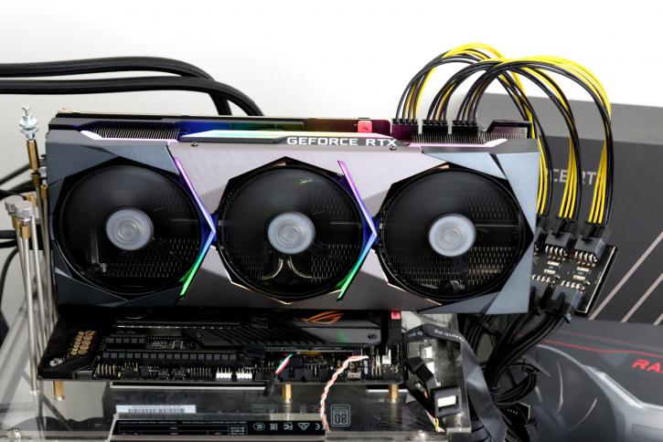
The GeForce RTX 3080 is based on the GA102-200 and 220 GPU and will get 8704 / 8960 Shader cores clocking in at 1710 MHz. This card sees 10GB of GDDR6X memory fitted, the new refresh model 12GB and it is running at 19 Gbps. So, that is a 320-bit or 384-bit wide bus, which is still a gnarly whopping 760/912 GB/s of memory bandwidth. Rated at a TGP of 320/350W, the card is connected with a 12-pin connector. The original Founder edition's 10GB cards have been released at a price of $699 USD. Currently you're lucky to spot one for 1500 USD.
GeForce RTX 3080 Ti
The GeForce RTX 3080 Ti is based on the GA102-225 GPU and will get 10240 Shader cores clocking in at a 1665 MHz boost frequency. This card sees 12GB of GDDR6X memory fitted and it is running at 19 Gbps. So, that is a 384-bit bus, which is still a mountainous 864 GB/s of memory bandwidth. Rated at a TGP of 350W, the card is connected with a 12-pin connector. With just these specifications, it should be pretty close to the GeForce RTX 3090 in performance. The Founder editions are released at a price of $1199 USD.
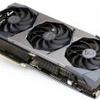
GeForce RTX 3090
The GeForce RTX 3090 comes with 24 GB of GDDR6X memory running on a 384-bit bus at 19.5 Gbps and that boils down to a frightful 936 GB/s of effective memory bandwidth. The GPU enabling it is the GA102-300 GPU, and it holds a comprehensive 10469 Shader cores. The clock frequency for the Shader cores will tick at 1695 MHz alongside a 350W rating on energy consumption, that's not a TDP. The TGP (Total Graphics Power) describes the maximum amount of graphics board power that the system power supply should be able to provide to the graphics card. The Founder editions are released at a price of $1499 USD.
 | |||||
|---|---|---|---|---|---|
| GeForce RTX 3090 | GeForce RTX 3080 Ti | GeForce RTS 3080 12GB | GeForce RTX 3080 10GB | Radeon RX 6900XT | |
| Architecture | Ampere | Ampere | Ampere | Ampere | RDNA2 |
| GPU | 8nm GA102-300 | 8nm GA102-225 | 8nm GA102-220 | 8nm GA102-200 | 7nm Navi 21 XTX |
| Transistors | 28.3 B | 28.3 B | 28.3 B | 28.3 B | 26.8 B |
| CU Clusters | 82 | 80 | 70 | 68 | 80 |
| Shader ores | 10496 | 10240 | 8960 | 8704 | 5120 |
| RT Cores | 82 | 80 | 70 | 68 | 80 |
| Tensor Cores | 328 | 320 | 280 | 272 | - |
| Texture Units | 328 | 320 | 280 | 272 | 320 |
| ROPs | 112 | 112 | 112 | 96 | 128 |
| Base Clock | 1395 MHz | 1365MHz | 1440 MHz | 1440 MHz | 1815 MHz |
| Boost Clock | 1695 MHz | 1665 MHz | 1710 MHz | 1710 MHz | 2250 MHz |
| Memory | 24 GB GDDR6X | 12 GDDRB G6X | 12 GB GDDR6X | 10 GB GDDR6X | 16GB GDDR6 |
| Memory Clock | 19.5 Gbps | 19 Gbps | 19 Gbps | 19 Gbps | 16 Gbps |
| Bandwidth | 936 GB/s | 912 GB/s | 912 GB/s | 760 GB/s | 512 GB/s |
| Memory Bus | 384-bit | 384-bit | 384-bit | 320-bit | 256-bit |
| TGP/TBP | 350W | 350W | 350W | 320W | 300W |
| MSRP | $1,499 | $1,199 | Not announced | $699 | $999 |
| Release Date | Sep 24th, 2020 | June 2nd, 2021 | January 2022 | Sep 17th, 2020 | Dec 8th, 2020 |
Ampere architecture
Ampere has an updated architecture that has gotten a new SM (Streaming Multiprocessor) design. One SM is a cluster that holds your Shader processors. As most of you have noticed, the Shader processor count was a bit of an enigma; it seems that mysteriously the Shader count has doubled up from what was expected in the first place. GA102/GA104 however contains three different types of compute cores:
- Programmable Shading Cores, which consist of Shader/Stream/CUDA Cores, Ampere received double the Shading capabilities.
- RT Cores, which accelerate Bounding Volume Hierarchy (BVH) traversal and intersection of scene geometry during ray-tracing, a gen 2 unit that now is twice as fast.
- Tensor Cores, which provide enormous speedups for AI neural network training and inferencing
The GPC is the dominant high-level hardware block with all of the key graphics processing units dwelling inside the GPC. Each GPC includes a dedicated Raster Engine, and now also includes two ROP partitions (each partition containing eight ROP units), which is a new feature for NVIDIA Ampere Architecture GA10x GPUs. The GPC includes six TPCs that each includes two SMs and one PolyMorph Engine. Each SM in GA10x GPUs then 128 Shading Cores, four third-generation Tensor Cores, a 256 KB Register File, four Texture Units, one second-generation ray-tracing core, and 128 KB of L1/Shared Memory, which can be configured for differing capacities depending on the needs of the compute or graphics workloads
So there would be further nuances to explain. Changes have been made to the Streaming Multiprocessor design that holds the Shading cores. The RTX 3000 series GPUs hold SMs that hold fp32 compute units. Ampere architecture supports parallel execution of FP32 and INT32 operations with independent thread scheduling. That's also described as concurrent execution of FP32 and INT32 operation. New, seen from Turing, is a combination of an INT32/FP32 cluster of Shader processors that effectively doubles up that Shader count.
Ampere is formed based on Graphics Processing Clusters (GPCs), Texture Processing Clusters (TPCs), Streaming Multiprocessors (SMs), Raster Operators (ROPS), and later the memory controllers. The GPC is the dominant high-level hardware block with all of the key graphics processing units residing inside the GPC. Each GPC includes a dedicated Raster Engine. Ampere has one more change here, it carries two ROP partitions (each partition containing eight ROP units), which is a new feature for NVIDIA Ampere Architecture GA10x GPUs.
PCI Express Gen 4.0
On the spec list is support for PCI-express 4.0. Competitor AMD had been making big bets with the 2019 NAVI products and already moved to PCIe Gen 4.0 as well as their chipsets and processors. But what does PCIe Gen 4.0 bring to the table? Well, simply put, more bandwidth for data to pass through.
|
PCIe Gen |
Line Code |
Transfer Rate |
x1 Bandwidth |
x4 |
x8 |
x16 |
|
1.0 |
8b/10b |
2.5 GT/s |
250 MB/s |
1 GB/s |
2 GB/s |
4 GB/s |
|
2.0 |
8b/10b |
5 GT/s |
500 MB/s |
2 GB/s |
4 GB/s |
8 GB/s |
|
3.0 |
128b/130b |
8 GT/s |
1 GB/s |
4 GB/s |
8 GB/s |
16 GB/s |
|
4.0 |
128b/130b |
16 GT/s |
2 GB/s |
8 GB/s |
16 GB/s |
32 GB/s |
|
5.0 |
128b/130b |
32 GT/s |
4 GB/s |
16 GB/s |
32 GB/s |
64 GB/s |
On the 4.0 interface, you’ll be hard-pressed to run out of bandwidth as each lane gets doubled up in that bandwidth, per lane. Of course, there has been a recent PCI-Express Gen 5.0 announcement as well, for ease of mind I already inserted it into the table. What benefits will you have at PCIe gen 4.0 with a graphics card? If we are to believe Nvidia's performance claims, the high-end RTX 3000 cards will probably benefit more from the new standard to make the most of the graphics memory buffers.
8K - AV1 - HDMI 2.1
New is active hardware-accelerated support for the new AV1 video compression standard. Ampere-based graphics cards can play back over their video decoder engine without utilizing your processor. NVIDIA specifically mentions decoder and not encoder. The NVENC API will not support encoding at this time. It has been talked about for a long time, but HDMI 2.1 is noted as a specification. The advantages of HDMI 2.1 are significant as the signal bandwidth can carry a lot over that HDMI cable (with a compatible display). HDMI 2.1 brings 144Hz support at a 4K resolution, as well as 60Hz at 8K.
