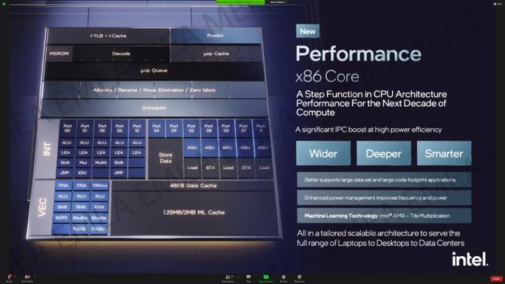
Architecture - Powerful Golden Cove cores - Intel AMX
Golden Cove performance cores
The architecture diagrams of the low-power Gracemont cores have just been presented to you, however, Alder Lake will make use of its Golden Cove CPU cores when speed and performance is critical. And these should make a significant difference in IPC when it comes to processing data compared to say Comet- and Rocket lake. Golden Cove CPU microarchitecture will take the place of the Sunny Cove, Willow Cove, and Cypress Cove microarchitectures, according to Intel. Originally described to as 10 nm Enhanced SuperFin, it will be made using Intel's Intel 7 manufacturing node, which was introduced in 2012. (10ESF). These high-performance cores will find their way into scalable processors such as Alder Lake and Xeon, as well as Sapphire Rapids.

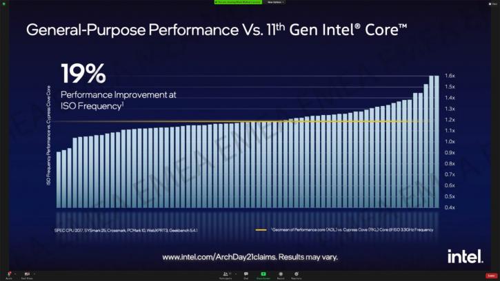
According to Intel, all of the enhancements combined should result in an improvement in IPC of 19 percent, which is on par with or slightly higher than the improvement achieved by Sunny Cove when compared to Skylake. That should even be sufficient to dethrone the Zen 3 architecture of the Ryzen 5000 CPUs.
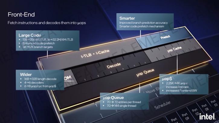
Intel has upgraded their vision; devote die space and power to improving performance on the front end. Notably, the micro-op cache, which is used to hold already-decoded instructions, has been enlarged to 4K. So for the frontend instructions can be lengthy and complex, here they are fetched and divided into what is called micro-ops, which are then used by the compute units to perform actual computation. To furhrt load up the hit rate of the micro-op cache, it can now store 4000 micro-ops as opposed to 2250 micro-ops. That's double of what it was and as an example, Haswell and Skylake did 1500 entries. Instructions are delivered swifter now but that creates another issue; processing (decoding) decoded must likewise be twice as fast. The number of decoders has been increased from four to six, and the length of instructions that can be decoded in a single clock tick has been increased from sixteen to thirty-two bytes, respectively.
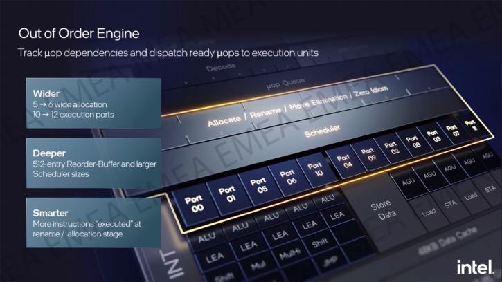
In the core backend, the actual math is done. In the Out-of-Order engine, the micro-ops are retrieved from the micro-opqueue and dispatched to the execution units as soon as all of the required variables have been determined by the system. The reorder buffer has been significantly increased from 352 to 512 entries.
Two new execution ports have been added to Golden Cove. In addition to the fifth alu port for integers, a new load port has been introduced, thus offering three load ports, each of which can handle a 256-bit load, or two 512-bit loads when used in conjunction.
The Golden Cove core, which will be used in Xeon CPUs, features an additional 2MB of L2 cache per core.
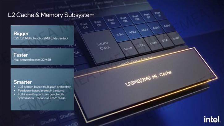
The memory subsystem is notable for getting more L2 cache per core - 1.25MB vs. 512KB.
IPC for the win.
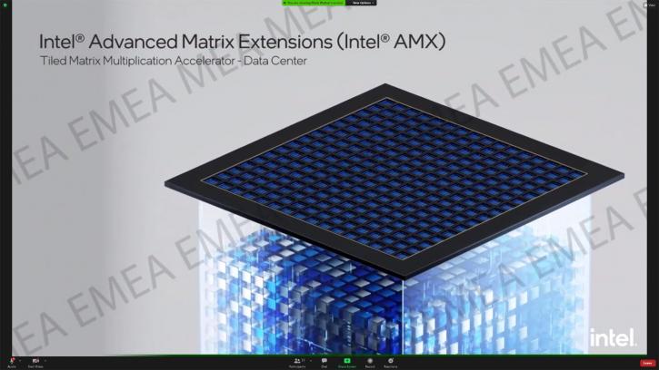
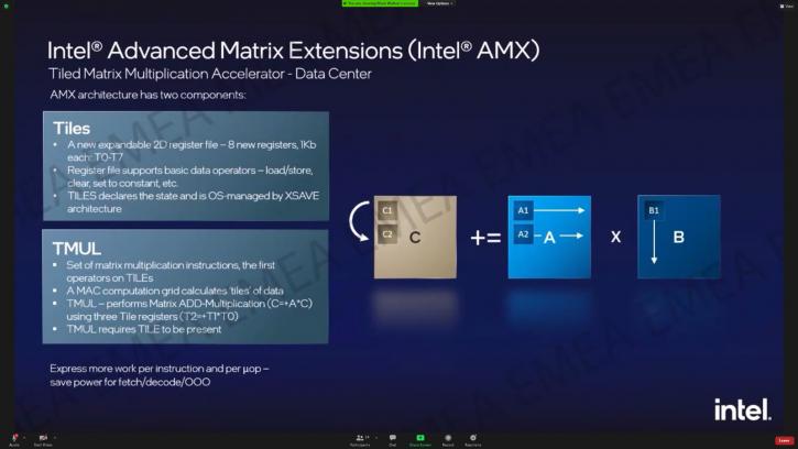
Intel AMX
A block called AMX will be seen on the CPU diagram, which is short for Advanced Matrix Extensions and is essentially equivalent to NVIDIA Tensor cores. AMX is short for Advanced Matrix Extensions, and it's practically a Tensor core replacement (tiled matrix multiplication accelerator). Targeted instruction can be used to run deal learning and artificial intelligence algorithms on these cores. The implementation of this for Alder Lake on a consumer level is currently unknown to us, as the presentation was obviously focused on the data center processing. Intel, on the other hand, is expected to take this step as it's definitely available in the processor.