Page 5
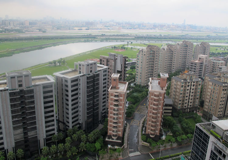
But the best thing yet is the magnificent view of Taipei from the 97 meters tall building alright.
Have a look at the second video please.
In this video we look at signal Digital Phosphor Oscilloscope, a unit that cost you a a couple of months of wages alright. if data signals in-between ICs do not work properly here's how they measure it. It helps in the debugging processes to track down design and component issues. This motherboard tested worked flawless by the way. Then we'll move towards other cubicles in on the R&D floor, showing some CAD designs (which we're probably not supposed to show), box design, further quality analysis units.
You'll spot lots and lots of motherboards, hardware like video cards being tested and a rather shy staff , especially when you point them at ... well a certain action figure (you'll understand when you see the video at 2:51 minutes).
The video ends at the roof top of the building, with the most brilliant overview of Taipei, we zoom in Taipei 101 -- but as stated it was rainy weather.
That's it for this small sneak peek into the ECS HQ - specifically the R&D floor. We appreciate ECS allowing us information frenzy journalist into the building with pretty much no restriction in our wicked scheme's of photo's shoots and video recording. We hope you enjoyed our behind the scenes look at ECS HQ in Taipei, Taiwan.
Remember, the really good stuff is inside the video's, should you have decided to skip them be sure to have a peek at them. This was our last coverage related towards Computex 2011, massive thanks out to ECS. Until next year.
- Leave/read comments
- Sign up to receive a notice when we publish a new article
- Or go back to Guru3D's front page
