Architecture and Specifications
Product overview
Vega 20 is being fabbed on the latest 7nm process technology, which is the densest foundry process available in an effort to reduce power consumption, die size and lower operating voltages. For the last six years, graphics processors have relied on 28nm high-k/metal nodes.
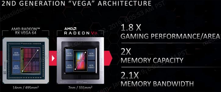
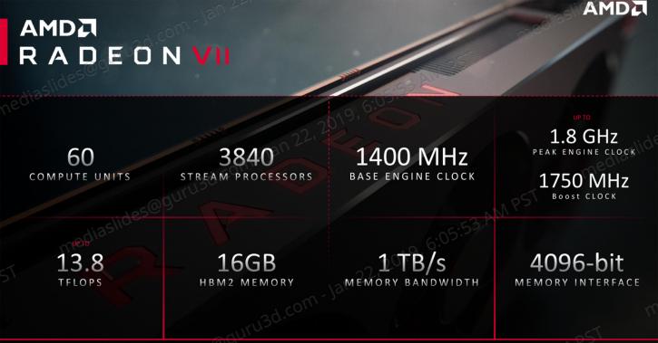
Two years ago we moved towards the last gen 14nm FinFET, and now we can half the size with 7nm node fabrication.Where Vega had a 56 and 64 edition, the Radeon VII will have just one card, fitted with 16 GB of HBM2 graphics memory, four stacks thus with a 4096-bit memory bus. The card as such will offer 1 TB/s of memory bandwidth. So when we break down the products in a more simplistic way we see the following:
 |
|||||
| AMD Radeon | Radeon VII | RX Vega 64 LCS | RX Vega 64 LE | RX Vega 56 | RX 580 |
| Graphics Core | Vega 20 | Vega 10 | Vega 10 | Vega 10 | Polaris 20 XTX |
| Fabrication Process | 7nm | 14 nm | 14 nm | 14 nm | 14 nm |
| Single Precision fp32 | 14.2 TFLOPs | 13.7 TFLOPs | 12.66 TFLOPs | 10.5 TFLOPs | 6.1 TFLOPs |
| Memory | 16GB HBM2 | 8GB HBM2 | 8GB HBM2 | 8 GB HBM2 | 4/8 GB GDDR5 |
| Clock Frequency Base / Boost |
1400 MHz 1750 MHz |
1,406 MHz 1,677 MHz |
1,247 MHz 1,546 MHz |
1,156 MHz 1,471 MHz |
1,257 MHz 1,340 MHz |
| Compute Units | 60 | 64 | 64 | 56 | 36 |
| Shader Processors | 3840 | 4096 | 4096 | 3584 | 2304 |
| Memory Interface | 4096-bit | 2048-bit | 2048-bit | 2048-bit | 256-bit |
| ROPs | 64 | 64 | 64 | 64 | 32 |
| TMUs | 240 | 256 | 256 | 224 | 144 |
| Memory Speed | 1000 MHz | 945 MHz | 945 MHz | 800 MHz | 8 Gbps |
| Memory Bandwidth | 1 TB/s | 484 GB/s | 484 GB/s | 410 GB/s | 256 GB/s |
| Board power | 300 W | 435 W | 295 W | 210 W | 185 W |
| MSRP | 699 USD | 600 USD | 499 USD | 399 USD | $199 (4 GB) $229 (8 GB) |
 |
|||||
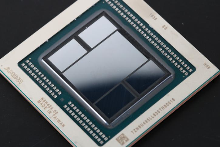
AMD has not unlocked the entire GPU, normally the Vega GPU is based on 64 shader clusters with 64 shader processors each. So that would make 4096 shader processors in total. AMD enabled 60 clusters (shader partitions), tied to 64 ROPs. TMUs wise for a fully enabled unit AMD has always used a 4:1 ratio meaning 60 CUs x 4 = 240 texture units.
|
Vega 64 Air cooled (64 CU Peak 1630MHz) |
Radeon VII (60 CU Peak 1800 MHz) |
MI60 (64 CU Peak 1800 MHz) |
|
|
Peak FP 64 |
0.84 TFLOPS |
3.46 TFLOPS |
7.4 TFLOPS |
|
Peak FP 32 |
13.4 TFLOPS |
13.8 TFLOPS |
14.7 TFLOPS |
|
Peak FP 16 |
26.7 TFLOPS |
27.7 TFLOPS |
29.5 TFLOPS |
|
Peak Int 8 |
53.4 TOPS |
55.3 TOPS |
59 TOPS |
|
Peak Int 4 |
106.8 TOPS |
110.7 TOPS |
118.0 TOPS |
Double precision (fp64), the cards are setup in a 1:4 ratio configuration for fp64. The Radeon VII graphics card was created for gamers and creators, enthusiasts and early adopters. AMD offers double precision compute performance to 3.46 TFLOPS (DP=1/4SP).
