Product Innards
Product Innards
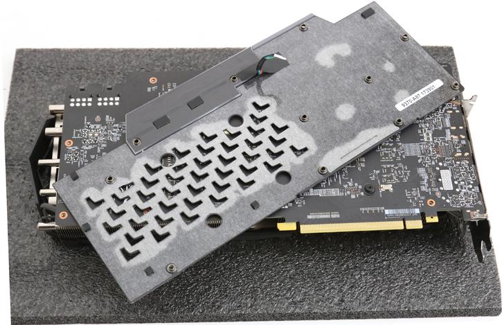
Here we take off the back-plate locked in with screws. At the top sits the RGB LED unit. As you can see the inside of the has enough spacing, regardless there is a nice plastic coating there, should for whatever reason a component ever hit the PCB, it would not short out.
Here we have removed the back-plate. That is an incredibly clean looking PCB for such a complex GPU alright. That is impressive to see.
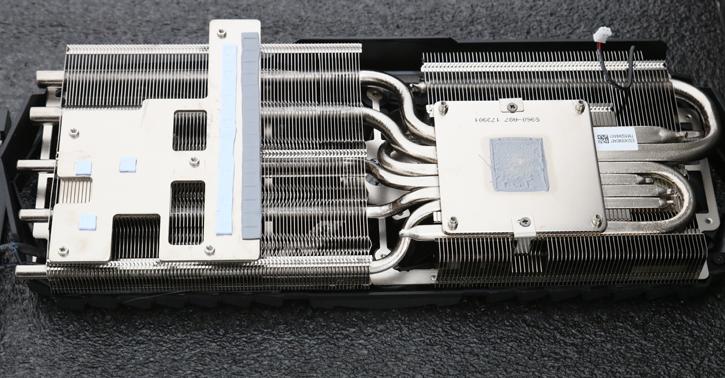
The cooling solution is pretty sweet overall, it uses many and very thick heat-pipes that pass through a heatsink, with thermal paste tied to the all-copper nickle plated block. It's different from the Lightning one, this one also covers the complete VRM area. Actually just based on what I see, I'd prefer this one over the Lightning block.
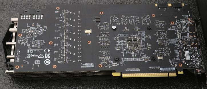
When we flip the PCB it around you can also see that the critical components are covered with a full contact plate. The memory area has padding as well as the phase chokes and thus is cooled. Again look how clean that PCB seems to be, very nice.
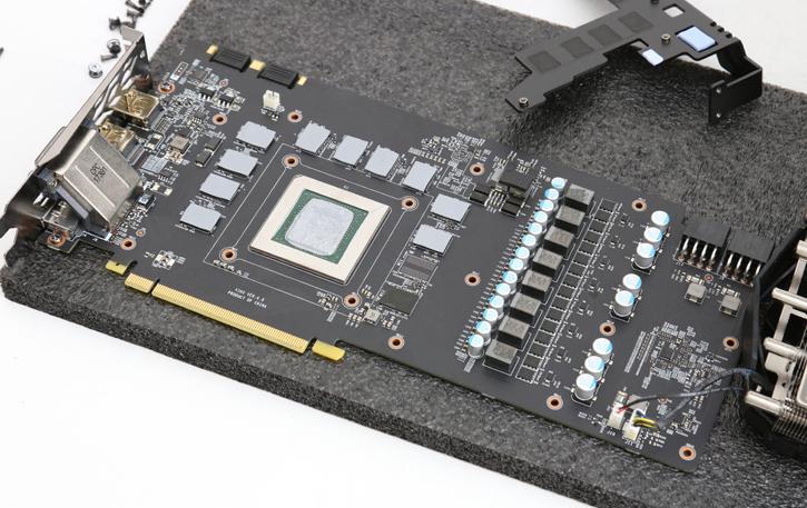
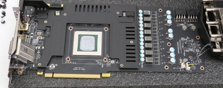
MSI did apply padding on top of the GDDR5X, the VRM area and parts as well. Here I have taken off the front and back-plates btw. There is roughly 2 mm space in between PCB and plate on the backside. We can now see the power stages, GPU, memory and voltage phase-controller.
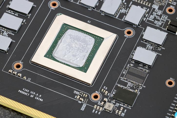
Here we have the front-side of the PCB, clearly visible the GP102 graphics processor from Nvidia covered with thermal interface material. The Nvidia GP102 graphics processor is made based on Pascal architecture at a 16 nm process at TSMC. This puppy has a transistor count of 12 billion and do not underestimate the die size, that is 471 mm² you are looking at.
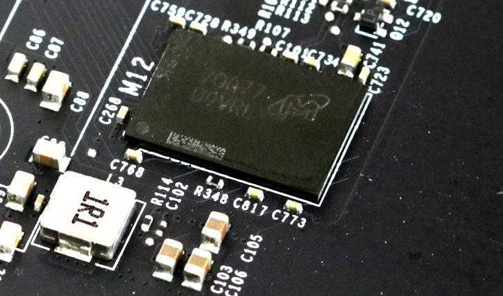
I had to saturate the photo to make the print readable. The GDDR5X memory chips are made by Micron and are specced to run at 11,000 MHz GDDR5 (effective data-rate). Tweaked, you are looking at a capability of roughly 12,000 MHz (effective data-rate). These are Micron D9VRL rated at 11 Gbps / 1.35V, however Micron also offers a 12 Gbps IC under the product name D9VRN. BTW That empty SMT trace on the previous photo is for another memory chip (cards that have 12 GB) like the Titan Xp.
The power phases for the graphics processor, removed now but everything is nicely cushioned with thermal padding reaching that cold-plate on the cooler.
I had to look and look and then look again. The photo as slightly out of focus and the inscription washed out due to thermal padding. Typically you'd see a uPI based uP9511P controller, however this is an OnSemi NCP81274 voltage controller. This is an eight phase buck controller regulator and thus allows for selectable 8/7/6/5/4/3/2/1 phases hence the board is doubling up phases (which is common).
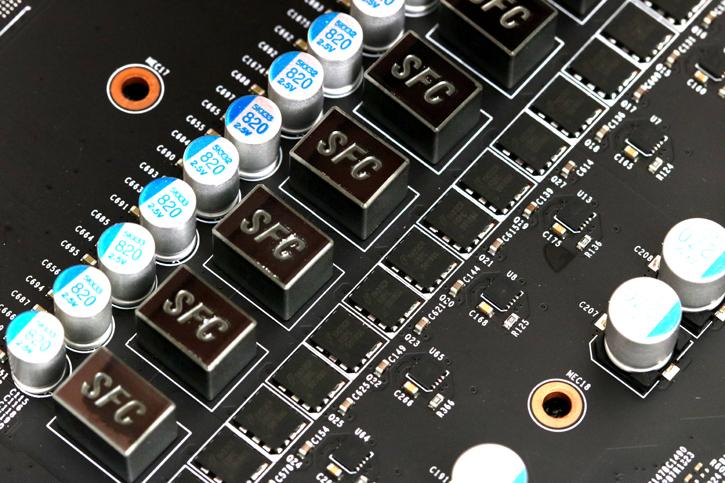
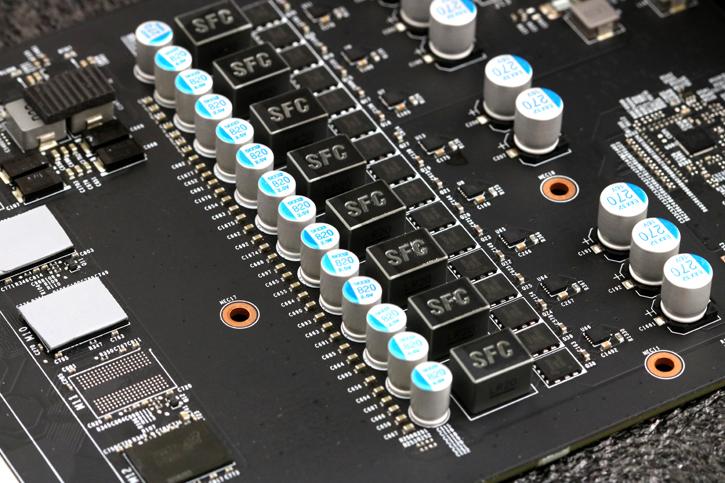
Across the PCB you see a clean component layout which includes premium VRM components. You can see SFC (Super Ferrite Choke) chokes which would be a molded inductor (chokes). These concrete alloy chokes help decreasing buzzing noises. And the the square chips to the right are mosfets.
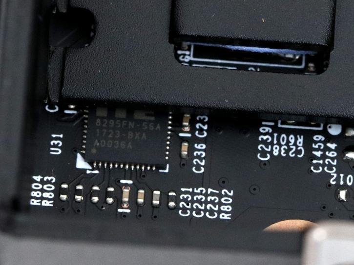
Oh hello there, all hiding, this chip right there is an 8295FN ITE, used for fan control.
