
The Falling Eagle
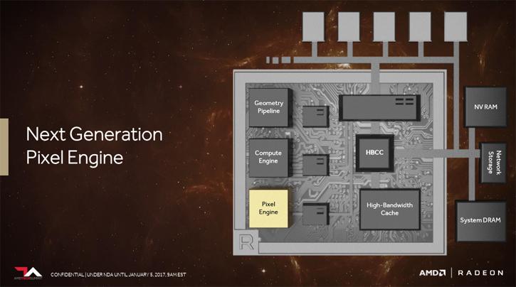
A new next generation pixel engine (output) has been designed to take memory efficiency to the next level. It includes a new rasterizer called draw stream binning rasterizer. There is something special happening with the pixel engine though. See that L1 cache sitting next to it ? Now look at the next screen-shot.
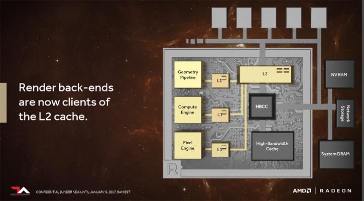
As you can see, the render back ends are now the clients of L2 cache as well, and not just the L1 buffers. This should/could greatly help deferred shading, a screen-space shading technique. It is called deferred because no shading is actually performed in the first pass of the vertex and pixel shaders: instead shading is "deferred" until a second pass. By making the render back-end clients of the L2 cache they get access to large pools in a much bigger buffer, the direct effect this has is in the end to improve in performance with applications that use deferred shading. So again here we should see an efficiency and thus performance increase.
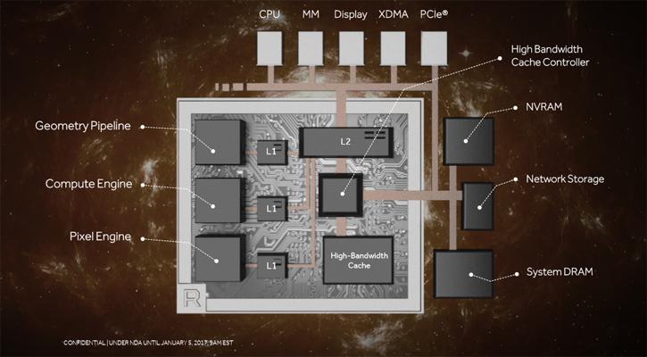
In the above screen-shot we can see VEGA in the form of a block diagram. We see a powerful GPU with a colossal architectural update. The move towards HBM2-type memory will give it the fast low latency bandwidth it needs, the new high bandwidth cache controller will make that bandwidth a fact, yet also can branch out and link towards your system memory, NVRAM yet also functions as interface towards many segments in that PC environment. All new is the programmable geometry pipeline, the CUs have received an update with programmable precision levels and finally the pixel engine got updated, the render back-end ties in towards the L2 cache again bringing performance enhancements.
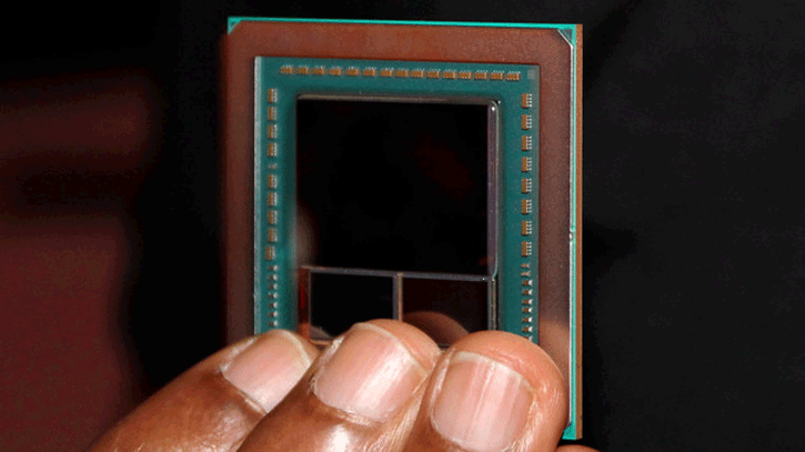
Above you can see (well almost) the a VEGA GPU.
Overall VEGA looks to be exciting, quite honestly though at this stage anything is uncertain. We still have to see actual values, numbers and results. The likelihood is great that it is however still a few months out from release for consumer products. Other than the screen-shots you see above AMD did not release any specifications in CU counts, clock freqeuencies memory volume etc. That remains secretive until closer to launch ... however ...
A bit of speculation
I am going to end with some discoveries at the event. At the event many topics have been shown including working samples of AMD VEGA.
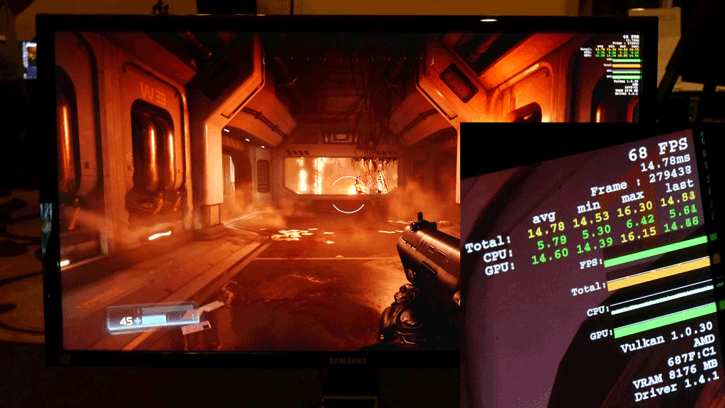
The photo shows a working VEGA setup in a demo room running Doom at ultra quality settings in an Ultra HD resolution, this was a demo room at the event. The photo comes from Golem.de and as explained is Doom running at 4K Ultra. The card is outing an FPS of 68 fps, with the "Vulkan" API enabled and what probably is a very early unoptimized engineering sample. That roughly is indicative for the performance of a GeForce GTX 1080.
A couple of things pop out, first off is the hardware device ID is revealed 687F:C1 and the second thing just has to be the graphics memory amount as the screenshot clearly is showing 8GB of HBM2 memory, with an estimated memory bandwidth of 512 GB/s. Back to the hardware ID, 687F:C1 anyone remember this post on AOTS?
If you like to have a look at the VEGA entire slide-deck from AMD, you can download it here.
- ATH +++
Hilbert out, peace.
