Over the weekend a lot of chatter started on the web and in our forums as at several sources report a new AMD SKU being in development. Basically AMD would be set to release a new graphics card that is lined up against the GTX 780 Ti to compete even better. The new product would use what is called HBM (high-bandwidth memory).
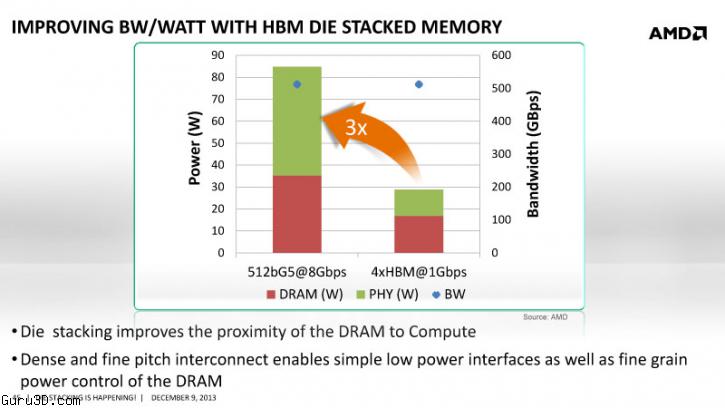
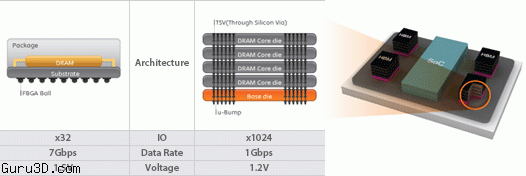
This is technology that uses multiple stacked DRAM dies with dedicated memory paths into a single package, cutting down on power-draw, thermals, and PCB materials. There three HBM memories availabke, 2Hi, 4Hi and 8Hi.
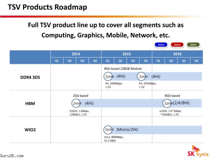
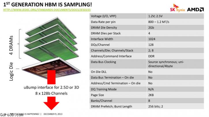
Now what we 'could' expect is say a product from the Volcanic Islands line being utilized with the first generation of HBM. The first variant to launch soon is 4Hi, which has a bandwidth of 128 GBps and four layers of DRAMs. Each module has 1GB of memory, so if you had 4 of them, then your bandwidth would be 512 GB/s.
The intersting thing is that a leaked document kind of shows the roadmap of future AMD GPUs. Thatb however is a complete shot in the dark. Volcanic Islands would be replaced with Pirate Islands somewhere in the second half of next year. Pirate Islands will be the first 20nm series. This basically means we are more than a year from now till 20nm node arrives from AMD. The 20nm process will not be our guest for long, AMD will quickly move forward to 14nm process with Pirate Islands Refresh.
- 28nm TSMC 1H 2014 : Hawaii, VI 1.0
- 28nm GlobalFoundries 2H 2014 : Iceland and Tonga, VI 2.0
- 28nm GlobalFoundries 1H 2015 : Maui, VI 2.0
- 20nm GlobalFoundries 2H 2015 : Fiji and Treasure, PI 1.0
- 20nm GlobalFoundries 1H 2016 : Bermuda, PI 1.0
- 14nm GlobalFoundries 2H 2016 : Mid-GPU and Low-GPU, PI 2.0
- 14nm GlobalFoundries 1H 2017 : High-GPU, PI 2.0
Will AMD Launch a new Single-GPU Card This Summer against GTX 780 Ti ?