SK Hynix Launches Fastest 8Gb Graphics DRAM (GDDR6) - Adopted by 2018
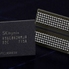
SK Hynix introduced the world’s fastest 2Znm 8Gb(Gigabit) GDDR6(Graphics DDR6) DRAM. The product operates with an I/O data rate of 16Gbps(Gigabits per second) per pin, which is the industry’s fastest. With a forthcoming high-end graphics card of 384-bit I/Os, this DRAM processes up to 768GB(Gigabytes) of graphics data per second.
SK Hynix has been planning to mass produce the product for a client to release high-end graphics card by early 2018 equipped with high performance GDDR6 DRAMs.
GDDR is specialized DRAM for processing an extensive amount of graphics data quickly according to what graphics cards command in PCs, workstations, video players and high performance gaming machines. Especially, GDDR6 is a next generation graphics solution under development of standards at JEDEC, which runs twice as fast as GDDR5 having 10% lower operation voltage. As a result, it is expected to speedily substitute for GDDR5 and GDDR5X. SK Hynix has been collaborating with a core graphics chipset client to timely mass produce the GDDR6 for the upcoming market demands.
“With the introduction of this industry’s fastest GDDR6, SK Hynix will actively respond to high quality, high performance graphics memory solutions market” said senior vice president Jonghoon Oh, the Head of DRAM Product Development Division. “The Company would help our clients enhance their performance of high-end graphics cards” he added.
GDDR6 is regarded as one of necessary memory solutions in growing industries such as AI(Artificial Intelligence), VR(Virtual Reality), self-driving cars, and high-definition displays over 4K to support their visualization. According to Gartner, average graphics DRAM density in graphics cards is to be 2.2GB this year and 4.1GB in 2021 with CAGR of 17%.
SK Hynix To Offer 72-Layer 3D NAND Flash - 04/10/2017 02:26 PM
SK Hynix introduced the industry's first 72-Layer 256Gb (Gigabit) 3D (Three-Dimensional) NAND Flash based on its TLC (Triple-Level Cell) arrays and own technologies. The company stacks 1.5 times more...
SK Hynix bids for Toshiba memory business - 02/07/2017 09:31 AM
South Korea's SK Hynix Inc has entered the running for a stake in Toshiba Corp's memory chip business, seeing an opportunity to gain on rivals in the booming NAND market, a person familiar with the ...
SK Hynix invests bigtime in new NAND memory factory - 12/23/2016 10:25 AM
Things are going well for memory manufacturer Hynix, they are investing massively in a new plant. In fact they will invest $2.6 billion to boost its NAND production to anticipate on increasing demand...
SK Hynix 8GHz 3D stackable GDDR5 memory - 11/18/2014 10:33 AM
Hynix started shipping its 3D stackable HBM (High-Bandwidth Memory) GDDR5 memory, stacked means more memory cells per IC. The chips have a capacity of 4Gb and are clocked at 8 Gbps. According to some,...
SK Hynix Develops 128 GB DDR4 Module - 04/08/2014 07:41 AM
Um, yeah you did read that right, 128 GB ! SK Hynix Inc. announced that it has developed the world's first highest density of 128 GB (Gigabytes) module based on 8 Gb(Gigabit) DDR4 using its advanced...
Senior Member
Posts: 495
Joined: 2017-02-04
Enjoy the ride until 2025.
Senior Member
Posts: 320
Joined: 2014-12-09
So Navi will come with GDDR6 i assume
Senior Member
Posts: 1396
Joined: 2004-02-14
Awesome! Yah I kinda figured GDDR6 would be the next step for most GPUs.
HBM2 is nice but it's damn expensive especially if you put more than 8GB on a card. With enthusiast class cards hitting 12GB it's very likely the next jump will be up to 14GB or 16GB.
With those larger memory sizes we'd need to see a jump in bus width too most likely. Probably 448-bit or 512-bit memory bus would be ideal for a card with that much memory. We haven't seen memory bus width like that since the GTX280 cards. lol
448-bit * 16000Mhz / 8 = 896GB/sec
512-bit * 16000Mhz / 8 = 1024GB/sec
Senior Member
Posts: 17410
Joined: 2009-02-25
So by looking up GDDR5 and HBM bandwidth then this "The product operates with an I/O data rate of 16Gbps(Gigabits per second) per pin, which is the industry’s fastest. With a forthcoming high-end graphics card of 384-bit I/Os, this DRAM processes up to 768GB(Gigabytes) of graphics data per second." means something like 96 GB/s per module? (8 GB so 8 * 96 = 768)
HBM1 (to compare.) being 128 GB/s but the Fury being classed as 512 GB/s due to 4 GB each using 128 so 128 * 4 = 512, I guess?
https://en.wikipedia.org/wiki/GDDR5-SDRAM
https://en.wikipedia.org/wiki/GDDR6-SDRAM
https://en.wikipedia.org/wiki/High-Bandwidth-Memory
Eh what do I know, faster and better than GDDR5 in any case.
(And probably cheaper than the upcoming HBM3 or what revision that was at now.)
EDIT: What's the TitanX(p) clocked at again, 12 GB/s with GDDR5X no? A nice little increase then for GDDR6 and then tweaked further by increasing the clock speed I suppose.
But what do I know, just thinking out loud trying to figure out the actual memory speed rather than the marketing text above using the product they tested and it's memory speed total.