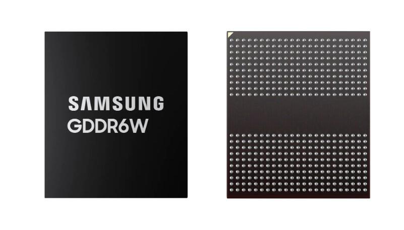
High performance, high capacity and high bandwidth memory solutions are helping bring the virtual realm to a closer match with reality. To meet this growing market demand, Samsung Electronics has developed GDDR6W (x64): the industry's first next-generation graphics DRAM technology.
GDDR6W builds on Samsung's GDDR6 (x32) products by introducing a Fan-Out Wafer-Level Packaging (FOWLP) technology, drastically increasing memory bandwidth and capacity.
Since its launch, GDDR6 has already seen significant improvements. Last July, Samsung developed a 24 Gbps GDDR6 memory, the industry's fastest graphics DRAM. GDDR6W doubles that bandwidth (performance) and capacity while remaining the identical size of GDDR6. Thanks to the unchanged footprint, new memory chips can easily be put into the same production processes customers have used for GDDR6, with the use of the FOWLP construction and stacking technology, cutting manufacturing time and costs.
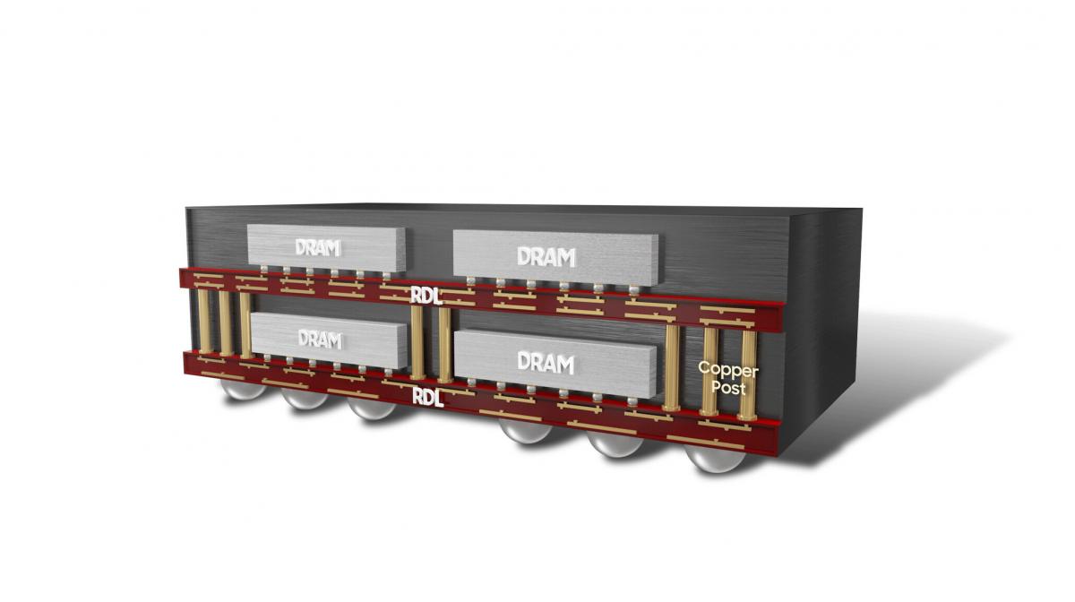
As shown in the picture below, since it can be equipped with twice as many memory chips in an identical size package, the graphic DRAM capacity has increased from 16Gb to 32Gb, while bandwidth and the number of I/Os has doubled from 32 to 64. In other words, the area required for memory has been reduced 50% compared to previous models.
Generally, the size of a package increases as more chips are stacked. But there are physical factors that limit the maximum height of a package. What's more, though stacking chips increases capacity, there is a trade-off in heat dissipation and performance. In order to overcome these trade-offs, we've applied our FOWLP technology to GDDR6W.
FOWLP technology directly mounts memory die on a silicon wafer, instead of a PCB. In doing so, RDL (Re-distribution layer) technology is applied, enabling much finer wiring patterns. Additionally, as there's no PCB involved, it reduces the thickness of the package and improves heat dissipation.
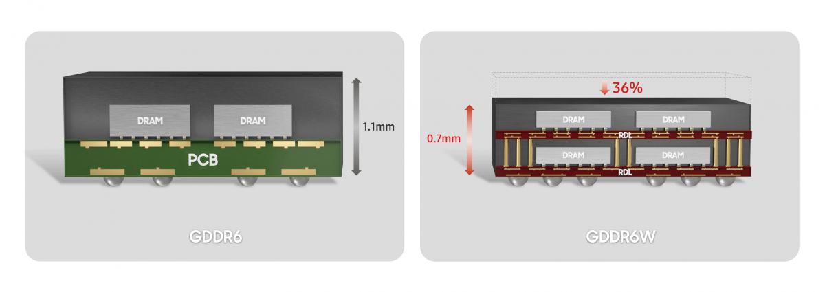
The height of the FOWLP-based GDDR6W is 0.7 mm - 36% slimmer than the previous package with a height of 1.1 mm. And despite the chip being multi-layered, it still offers the same thermal properties and performance as the existing GDDR6. Unlike GDDR6, however, the bandwidth of the FOWLP-based GDDR6W can be doubled thanks to the expanded I/O per single package.
Packaging refers to the process of cutting fabricated wafers into semiconductor shapes or connecting wires. In the industry, this is known as a 'back-end process.' While the semiconductor industry has continuously developed towards scaling circuits as much as possible during the front-end process, packaging technology is becoming more and more important as the industry approaches the physical limits of chip sizes limits. That's why Samsung is using its 3D IC package technology in GDDR6W, creating a single package by stacking a variety of chips in a wafer state. This is one of many innovations planned to make advanced packaging for GDDR6W faster and more efficient.
The newly developed GDDR6W technology can support HBM-level bandwidth at a system level. HBM2E has a system-level bandwidth of 1.6 TB/s based on 4K system-level I/O and a 3.2 Gbps transmission rate per pin. GDDR6W, on the other hand, can produce a bandwidth of 1.4 TB/s based on 512 system-level I/O and a transmission rate of 22Gpbs per pin. Furthermore, since GDDR6W reduces the number of I/O to about 1/8 compared with using HBM2E, it removes the necessity of using microbumps. That makes it more cost-effective without the need for an interposer layer.