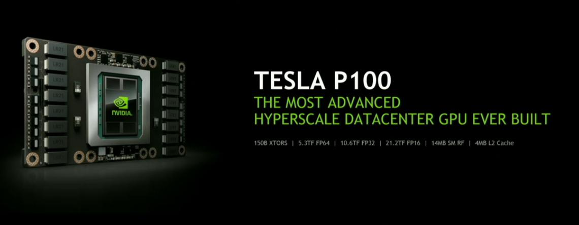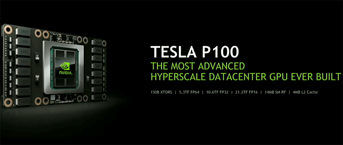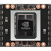
Nvidia just announced a HPC data-center module based on Pascal GPU architecture. The Tesla P100 is a daughter add-in board that holds 150B transistors, the GPU itself however will hold 15B transistors.
The Tesla P100 will be based on Pascal architecture and is fabbed at 16nm FinFet design and comes with stacked HBM2 (16GB likely in four stacks). The Pascal based GPU driving the unit holds 15 Billion transistors which is roughly double that of the current biggest Maxwell chip. If I heard it right in the keynote the primary Pascal based GPU is huge at 600mm^2.
The prognosis performance (according to Nvidia) is 5.3TFLOPS using 64-bit floating-point numbers and is rated at 10.6TFLOPS using 32-bit and 21.2TFLOPS using 16-bit. P100 has 4MB of L2 cache and 14MB of shared memory for just the register file.
The following table provides a high-level comparison of Tesla P100 specifications compared to previous-generation Tesla GPU accelerators.
| Tesla Products | Tesla K40 | Tesla M40 | Tesla P100 |
| GPU | GK110 (Kepler) | GM200 (Maxwell) | GP100 (Pascal) |
| SMs | 15 | 24 | 56 |
| TPCs | 15 | 24 | 28 |
| FP32 CUDA Cores / SM | 192 | 128 | 64 |
| FP32 CUDA Cores / GPU | 2880 | 3072 | 3584 |
| FP64 CUDA Cores / SM | 64 | 4 | 32 |
| FP64 CUDA Cores / GPU | 960 | 96 | 1792 |
| Base Clock | 745 MHz | 948 MHz | 1328 MHz |
| GPU Boost Clock | 810/875 MHz | 1114 MHz | 1480 MHz |
| FP64 GFLOPs | 1680 | 213 | 5304 |
| Texture Units | 240 | 192 | 224 |
| Memory Interface | 384-bit GDDR5 | 384-bit GDDR5 | 4096-bit HBM2 |
| Memory Size | Up to 12 GB | Up to 24 GB | 16 GB |
| L2 Cache Size | 1536 KB | 3072 KB | 4096 KB |
| Register File Size / SM | 256 KB | 256 KB | 256 KB |
| Register File Size / GPU | 3840 KB | 6144 KB | 14336 KB |
| TDP | 235 Watts | 250 Watts | 300 Watts |
| Transistors | 7.1 billion | 8 billion | 15.3 billion |
| GPU Die Size | 551 mm² | 601 mm² | 610 mm² |
| Manufacturing Process | 28-nm | 28-nm | 16-nm |
The GFLOPS in this chart are based on GPU Boost Clocks.
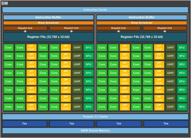
GP100’s SM incorporates 64 single-precision (FP32) CUDA Cores. In contrast, the Maxwell and Kepler SMs had 128 and 192 FP32 CUDA Cores, respectively. The GP100 SM is partitioned into two processing blocks, each having 32 single-precision CUDA Cores, an instruction buffer, a warp scheduler, and two dispatch units. While a GP100 SM has half the total number of CUDA Cores of a Maxwell SM, it maintains the same register file size and supports similar occupancy of warps and thread blocks.
GP100’s SM has the same number of registers as Maxwell GM200 and Kepler GK110 SMs, but the entire GP100 GPU has far more SMs, and thus many more registers overall. This means threads across the GPU have access to more registers, and GP100 supports more threads, warps, and thread blocks in flight compared to prior GPU generations.
Each SM has 64 CUDA cores and four texture units, that's 3840 shader cores and 240 texture units.
The product is samples already to IBM, HP, Dell and Cray. Tesla P100 servers will be be coming in Q1 2017. These will be used for AI, Cloud functionality and deep learning. Nvidia announced that the P100 is going into production as we speak, which is interesting considering it is using HBM2.
Tesla P100 Specifications
Specifications of the Tesla P100 GPU accelerator include:
- 5.3 teraflops double-precision performance, 10.6 teraflops single-precision performance and 21.2 teraflops half-precision performance with NVIDIA GPU BOOST™ technology
- 160GB/sec bi-directional interconnect bandwidth with NVIDIA NVLink
- 16GB of CoWoS HBM2 stacked memory
- 720GB/sec memory bandwidth with CoWoS HBM2 stacked memory
- Enhanced programmability with page migration engine and unified memory
- ECC protection for increased reliability
- Server-optimized for highest data center throughput and reliability
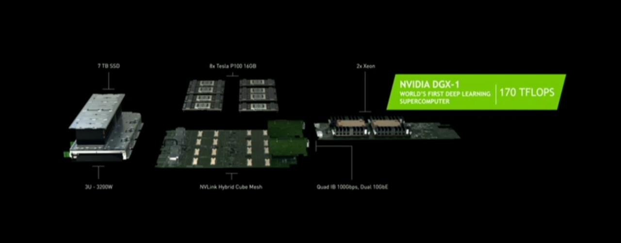
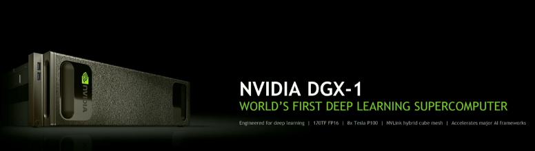
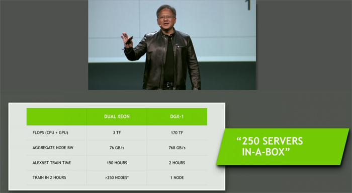
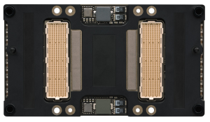
Parallel to the P100 announcement Nvidia is announcing the DGX-1, a deep learning super computer. It holds two Xeon processors and a lovely eight Tesla P100 units each holding 16GB of HBM2 memory. Priced at only $129,000, but it is considered to be a super-computer.
Obviously P100 will be the base model GPU wise that will empower future graphics cards.
It is interesting to see this announcement as it indicates that despite what was announced, HBM2 memory is already available. I'll add more info and specs as (and if) they arrive.
--
Press release added
--
SAN JOSE, CA--(Marketwired - Apr 5, 2016) - GPU Technology Conference -- NVIDIA (NASDAQ: NVDA) today introduced the NVIDIA® Tesla® P100 GPU, the most advanced hyperscale data center accelerator ever built.
The latest addition to the NVIDIA Tesla Accelerated Computing Platform, the Tesla P100 enables a new class of servers that can deliver the performance of hundreds of CPU server nodes. Today's data centers -- vast network infrastructures with numerous interconnected commodity CPU servers -- process large numbers of transactional workloads, such as web services. But they are inefficient at next-generation artificial intelligence and scientific applications, which require ultra-efficient, lightning-fast server nodes.
Based on the new NVIDIA Pascal™ GPU architecture with five breakthrough technologies, the Tesla P100 delivers unmatched performance and efficiency to power the most computationally demanding applications.
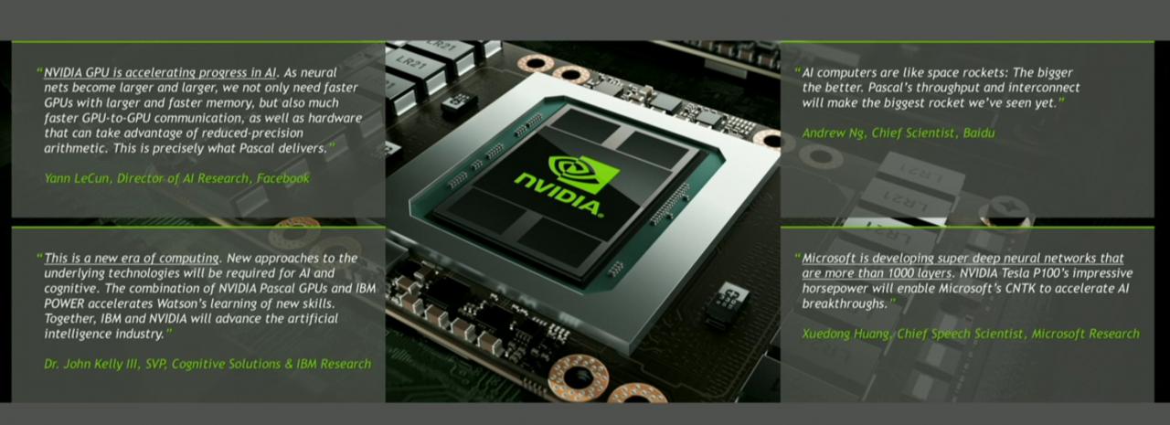
"Our greatest scientific and technical challenges -- finding cures for cancer, understanding climate change, building intelligent machines -- require a near-infinite amount of computing performance," said Jen-Hsun Huang, CEO and co-founder, NVIDIA. "We designed the Pascal GPU architecture from the ground up with innovation at every level. It represents a massive leap forward in computing performance and efficiency, and will help some of the smartest minds drive tomorrow's advances."
Dr. John Kelly III, senior vice president, Cognitive Solutions and IBM Research, said: "As we enter this new era of computing, entirely new approaches to the underlying technologies will be required to fully realize the benefits of AI and cognitive. The combination of NVIDIA GPUs and OpenPOWER technology is already accelerating Watson's learning of new skills. Together, IBM's Power architecture and NVIDIA's Pascal architecture with NVLink will further accelerate cognitive workload performance and advance the artificial intelligence industry."
Five Architectural Breakthroughs
The Tesla P100 delivers its unprecedented performance, scalability and programming efficiency based on five breakthroughs:
- NVIDIA Pascal architecture for exponential performance leap -- A Pascal-based Tesla P100 solution delivers over a 12x increase in neural network training performance compared with a previous-generation NVIDIA Maxwell™-based solution.
- NVIDIA NVLink for maximum application scalability -- The NVIDIA NVLink™ high-speed GPU interconnect scales applications across multiple GPUs, delivering a 5x acceleration in bandwidth compared to today's best-in-class solution1. Up to eight Tesla P100 GPUs can be interconnected with NVLink to maximize application performance in a single node, and IBM has implemented NVLink on its POWER8 CPUs for fast CPU-to-GPU communication.
- 16nm FinFET for unprecedented energy efficiency -- With 15.3 billion transistors built on 16 nanometer FinFET fabrication technology, the Pascal GPU is the world's largest FinFET chip ever built2. It is engineered to deliver the fastest performance and best energy efficiency for workloads with near-infinite computing needs.
- CoWoS with HBM2 for big data workloads -- The Pascal architecture unifies processor and data into a single package to deliver unprecedented compute efficiency. An innovative approach to memory design, Chip on Wafer on Substrate (CoWoS) with HBM2, provides a 3x boost in memory bandwidth performance, or 720GB/sec, compared to the Maxwell architecture.
- New AI algorithms for peak performance -- New half-precision instructions deliver more than 21 teraflops of peak performance for deep learning.
The Tesla P100 GPU accelerator delivers a new level of performance for a range of HPC and deep learning applications, including the AMBER molecular dynamics code, which runs faster on a single server node with Tesla P100 GPUs than on 48 dual-socket CPU server nodes3. Training the popular AlexNet deep neural network would take 250 dual-socket CPU server nodes to match the performance of eight Tesla P100 GPUs4. And the widely used weather forecasting application, COSMO, runs faster on eight Tesla P100 GPUs than on 27 dual-socket CPU servers5.
The first accelerator to deliver more than 5 and 10 teraflops of double-precision and single-precision performance, respectively, the Tesla P100 provides a giant leap in processing capabilities and time-to-discovery for research across a broad spectrum of domains.