Guru3D.com
  • HOME
  • NEWS
    • Channels
    • Archive
  • DOWNLOADS
    • New Downloads
    • Categories
    • Archive
  • GAME REVIEWS
  • ARTICLES
    • Rig of the Month
    • Join ROTM
    • PC Buyers Guide
    • Guru3D VGA Charts
    • Editorials
    • Dated content
  • HARDWARE REVIEWS
    • Videocards
    • Processors
    • Audio
    • Motherboards
    • Memory and Flash
    • SSD Storage
    • Chassis
    • Media Players
    • Power Supply
    • Laptop and Mobile
    • Smartphone
    • Networking
    • Keyboard Mouse
    • Cooling
    • Search articles
    • Knowledgebase
    • More Categories
  • FORUMS
  • NEWSLETTER
  • CONTACT

New Reviews
Corsair RM1200X SHIFT 1200W PSU Review
Intel NUC 13 Pro (Arena Canyon) review
Endorfy Arx 700 Air chassis review
Beelink SER5 Pro (Ryzen 7 5800H) mini PC review
Crucial T700 PCIe 5.0 NVMe SSD Review - 12GB/s
Sapphire Radeon RX 7600 PULSE review
Gainward GeForce RTX 4060 Ti GHOST review
Radeon RX 7600 review
ASUS GeForce RTX 4060 Ti TUF Gaming review
MSI GeForce RTX 4060 Ti Gaming X TRIO review

New Downloads
CrystalDiskInfo 9.0.1a Download
AMD Radeon Software Adrenalin 23.5.2 WHQL download
Intel ARC graphics Driver Download Version: 31.0.101.4382
Corsair Utility Engine Download (iCUE) Download v5.2
GeForce 535.98 WHQL driver download
CPU-Z download v2.06
AMD Radeon Software Adrenalin 23.5.1 WHQL download
GeForce 532.03 WHQL driver download
AMD Chipset Drivers Download 5.05.16.529
Display Driver Uninstaller Download version 18.0.6.4


New Forum Topics
Third party Graphics Card hardware database Extreme 4-Way Sli Tuning AMD's Future Developments: Ryzen 8000 and Navi 3.5 PSA: 535 system stability concerns. Nvidia Driver & COD MW2 NVIDIA GeForce Hotfix Driver 536.09 Researchers Expose Vulnerabilities in AMD's Firmware-Based TPMs Seby9123 Emerges as OC Champion in G.SKILL OC World Cup 2023 AMD EPYC 7002 Server Processors Reportedly Harbour a Bug - Crashes After 1044 Days of Uptime ASRock to Launch the MicroATX Motherboard B650M Pro RS


Guru3D.com » News » NVIDIA Ampere GA102-300-A1 GPU (GeForce RTX 3090) Caught on Camera

NVIDIA Ampere GA102-300-A1 GPU (GeForce RTX 3090) Caught on Camera

by Hilbert Hagedoorn on: 08/25/2020 05:06 PM | source: chiphell (via Videocardz) | 36 comment(s)
NVIDIA Ampere GA102-300-A1 GPU (GeForce RTX 3090) Caught on Camera

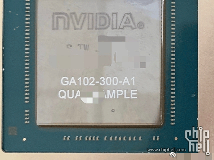
Check it out, the first photo of an NVIDIA "Ampere" GA102 graphics processor chip aka the GPU that is to fire up the GeForce RTX 3090. Over in Asia in the Chiphell forums this got posted, and it's the real deal.

You'll notice qual sample. Meaning it was a validation/engineering sample chip. Looking at the size of that puppy, it'll hold many MANY transistors as that die is based on 7nm fabrication. The GA102-300-A1 would be firing the GeForce RTX 3090 and is expected to get a Shader count of 5,248 units. All that tied towards 24GB of GDDR6X graphics memory running in a ~19 Gbps realm. It is expected that this is the product that NVIDIA will announce its Ampere cards on the 1st of September, perhaps they'll announce 10GB GeForce RTX 3080 cards that day as well. Chatter on the street is that the latter will initially be launched at 10GB GDDR6X with later on a 20GB model. It is all chatter though as to date NVIDIA has not been talking Ampere with media whatsoever.


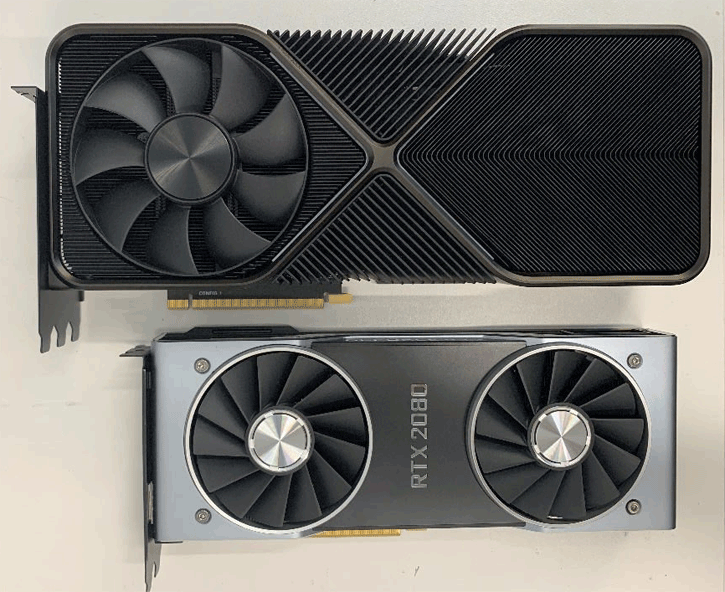
Earlier on a Twitter use named @GarnetSunset posted the photos below the fold. The NVIDIA GeForce RTX 3090 as a graphics card is going to be big alright, as the way I see it, that's three slots.  The name of the card has been blurred out. GeForce RTX 3090 us rumored to have a GA102-300-A1 GPU armed with 5,248 shader processors spread over 82 SMs. And likely that is still not a fully enabled chip :-)

The card would get a massive 24 GB of memory connected throughout a 384-bit wide memory bus based on high-bandwidth GDDR6X. This leaker also mentioned a price of 1400 USD, much like the leak we have seen earlier this week. 


NVIDIA Ampere GA102-300-A1 GPU (GeForce RTX 3090) Caught on Camera


« Corsair offers Two New Custom Cooling Simple Hydro X Series Starter Kits · NVIDIA Ampere GA102-300-A1 GPU (GeForce RTX 3090) Caught on Camera · NVIDIA announces GeForce MX450 laptop video card with pci-e 4.0 and gddr6 »

Related Stories

NVIDIA Announces Financial Results for Second Quarter Fiscal 2021 - 08/20/2020 08:29 AM
NVIDIA today reported record revenue for the second quarter ended July 26, 2020, of $3.87 billion, up 50 percent from $2.58 billion a year earlier, and up 26 percent from $3.08 billion in the previous...

NVIDIA Ampere cards well under way for a release in September? Flagship 50% faster? - 08/03/2020 11:22 AM
Judging from all signals in the industry, NVIDIA is now really close to release their first consumer-based Apere graphics cards. Indicated is an announcement late August, and release in late September...

ASUS Announces ESC4000A-E10 Server Powered by the NVIDIA A100 PCIe GPU - 06/23/2020 08:37 AM
ASUS announced ESC4000A-E10, a new GPU server powered by the NVIDIA A100 PCIe® GPU and featuring PCIe 4.0 expansion and OCP 3.0 networking....

NVIDIA announces A100 PCIe accelerator - 06/22/2020 01:26 PM
NVIDIA and the world’s leading server manufacturers today announced NVIDIA A100-powered systems in a variety of designs and configurations to tackle the most complex challenges in AI, data science a...

NVIDIA Announces Financial Results for First Quarter Fiscal 2021 - 05/22/2020 08:16 AM
NVIDIA today reported revenue for the first quarter ended April 26, 2020, of $3.08 billion, up 39 percent from $2.22 billion a year earlier, and down 1 percent from $3.11 billion in the previous quart...


8 pages 1 2 3 4 > »


Cidious
Senior Member


Posts: 150
Joined: 2007-11-13

#5821649 Posted on: 08/25/2020 05:25 PM
@Hilbert Hagedoorn: Where did you find it's made on 7nm? the reports are that it's Samsung's 8nm (10nm+). Suddenly you report it's 7nm without a valid source. I would like the see the source for this.

Astyanax
Senior Member


Posts: 15722
Joined: 2018-03-21

#5821651 Posted on: 08/25/2020 05:26 PM
@Hilbert Hagedoorn: Where did you find it's made on 7nm? the reports are that it's Samsung's 8nm (10nm+). Suddenly you report it's 7nm without a valid source. I would like the see the source for this.


the made in TW stamp on it.......

XenthorX
Senior Member


Posts: 4718
Joined: 2014-06-17

#5821652 Posted on: 08/25/2020 05:26 PM
TW= Taiwan/TSMC 7nm ?

erho
Member


Posts: 35
Joined: 2018-09-02

#5821655 Posted on: 08/25/2020 05:36 PM
the made in TW stamp on it.......

Some TU102/TU104 chips have "Korea" stamped on them but they are all made in TSMC, Taiwan. I think that stamp is related to packaging/assembly, not foundry.


Denial
Senior Member


Posts: 14091
Joined: 2004-05-16

#5821656 Posted on: 08/25/2020 05:37 PM
Yeah, it's usually stamped where the package is assembled and not where the die is fabricated.

8 pages 1 2 3 4 > »


Post New Comment
Click here to post a comment for this news story on the message forum.


Guru3D.com © 2023