Intel to fab Meteor Lake Die on Intel 4 Node / 20% higher clocks
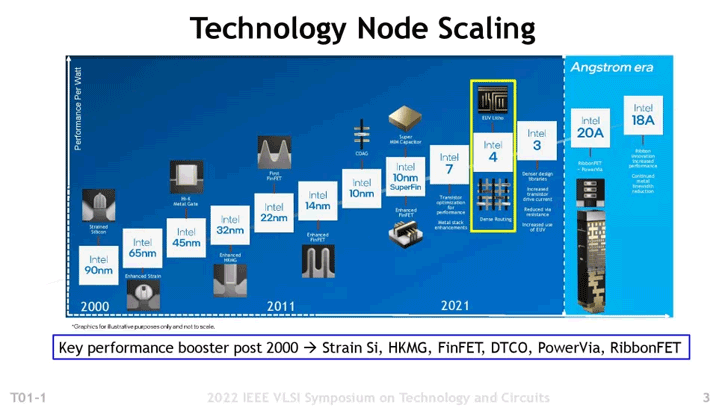
Intel has next level and gen Intel 4-chip technology in the works, Meteror Lake CPU clock rates will be are 20+% faster while keeping the same TDPs. Intel 4 is the first chip node where euv chip machines are used. Intel also demonstrated a dieshot of a Meteor Lake processor.
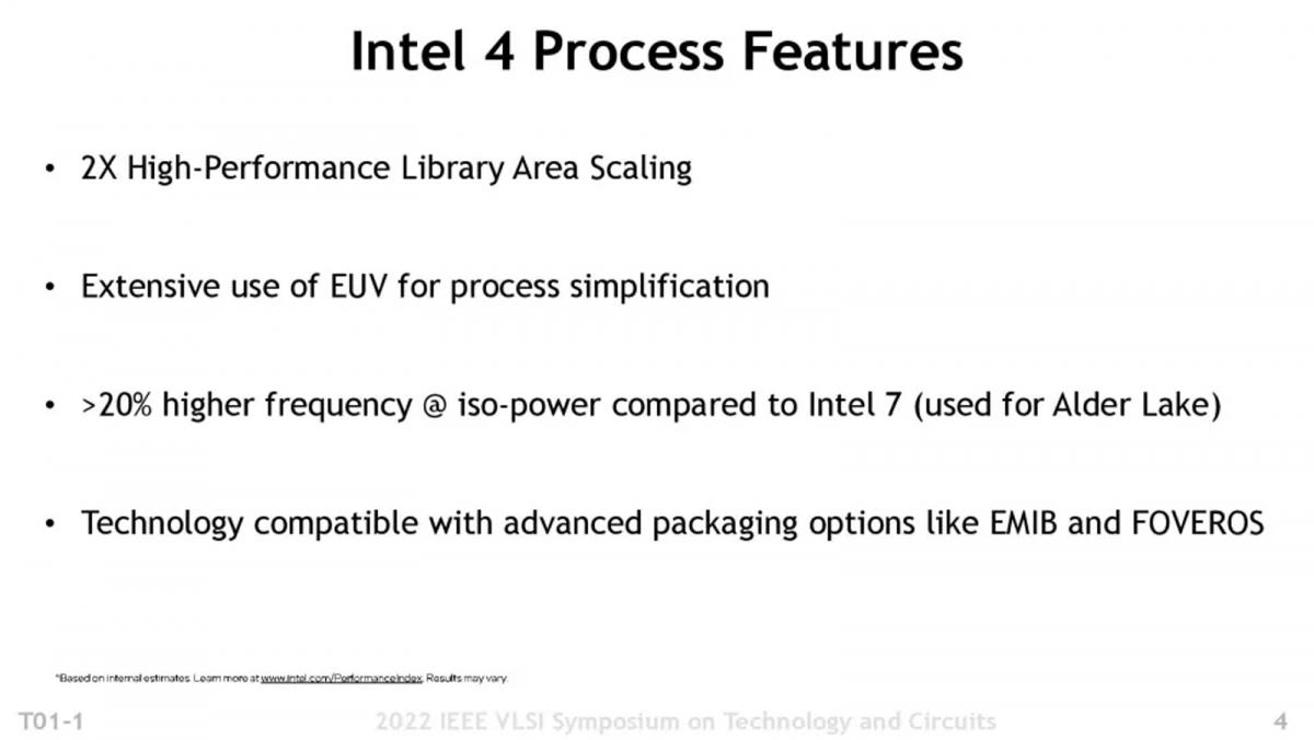
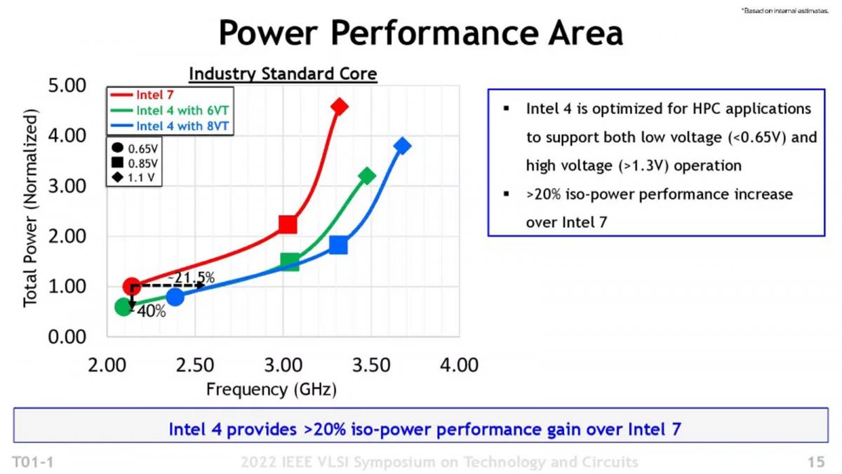
Intel revealed at the IEEE VLSI Symposium 2022 that Intel 4 allows 21.5 percent higher clock speeds at the same tdp, 40 percent lower energy consumption at the same clock speeds, or a combination thereof. Tom's Hardware discusses the presentation in an article.
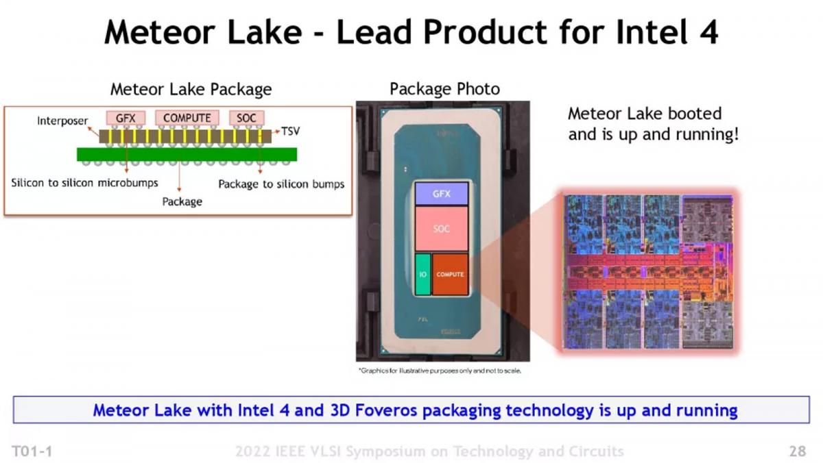
Intel is creating many nodes concurrently in order to meet its promise of delivering five nodes in four years, and Intel 4 is the second step in that journey. Let's start with a closer look at the Meteor Lake die, then get into the specifics of the I4 presentation. Meteor Lake from Intel will be the first product to use the I4 technology. Meteor Lake is expected to be released in 2023, according to Intel. Meteor Lake will employ Intel's 3D stacking packaging technology, as seen with Lakefield chips. This will, however, be Intel's first step into high-volume manufacturing with this cutting-edge packaging technology.
TSV connectors will be used to connect the four die (referred to as 'tiles' in Intel nomenclature) to an interposer. Intel has not revealed whether this interposer will be active or passive, or whether it will house caches or other control circuits. The computing tile, I/O tile, SOC tile, and graphics tile will be mounted on this interposer by Intel. Intel has stated that the computation tile will use I4, but has not indicated which nodes would be used for the remaining tiles. TSMC's N3 (3nm) node with the Meteor and Arrow Lake CPUs was listed on a slide in the above album during the company's Analyst Day earlier this year. This is often assumed to be the graphical tile. Only time will tell.
Meteor Lake chips, like Alder Lake, have an x86 hybrid architecture. We have six p-cores and eight e-cores in this example. On the left of the compute die, we can see six blue-colored Redwood Cove performance cores (p-cores), which are used for latency- and performance-sensitive operations. On the right, we observe two purple four-core clusters of Crestmont efficiency cores (e-cores). Background and multi-threaded work are handled by these cores. The L3 caches and connectivity circuitry are located in the chip's core. Intel has yet to provide a further description of the differences between the SoC and I/O tiles, with the former a likely candidate for memory controllers and PCIe interfaces, while the latter could be for Thunderbolt and other PCH-types of interfaces. Because the I4 node is forward compatible with the I3, designs can be switched between the two without going through the time-consuming porting process. Intel claims that the I4's successor, dubbed 'Intel 3,' will include both high-performance and high-density libraries. To further simplify the design, the I3 process will include improved transistors and interconnects, as well as more EUV layers. The I3 node will be 18% quicker than the I4 node and will be the first new node offered by Intel through Intel Foundry Services (IFS) (the company already offers its existing 16nm).
Alder Lake-X mentioned in AIDA64 - Intel to return to the HEDT market? - 04/11/2022 09:20 AM
AIDA build 64 6.60.5944 patch notes indicate preliminary compatibility for a mysterious new Intel CPU platform called Alder Lake-X. This suggests that Intel is returning to the HEDT market after a lon...
Intel to Demonstrate Arc Ray-Tracing and XeSS Technology at GDC 2022 - 03/15/2022 10:01 AM
Intel will utilize this year's Games Developers Conference (GDC) to reveal details about its new Arc Alchemist graphics card line. Intel will present a number of talks at GDC pertaining to ray tracin...
Rumor: Intel To Release Six Alder Lake Processors for Desktops Nov. 4 Pre-orders Start October 27 - 10/18/2021 06:36 PM
On November 4, it appears to have been verified that Intel's first Alder Lake processors will be available for purchase. Alder Lake review embargoes will expire on that day, and sales of these chips ...
Intel to disable insecure TSX feature on older CPUs - 06/30/2021 08:23 AM
Intel has decided to deactivate Transactional Sync Extensions in Skylake, Kaby Lake, Coffee Lake and Whiskey Lake processor chips. Intel deactivates the feature because of memory ordening errors and ....
Intel To Host COMPUTEX 2021 Opening Keynote: Innovation Unleashed - 05/19/2021 08:51 AM
Join Intel Executive Vice President Michelle Johnston Holthaus for Intel's first virtual COMPUTEX keynote and a firsthand look at how the strategies of new CEO Pat Gelsinger, along with the forces of...
Senior Member
Posts: 119
Joined: 2003-07-29
Well, they actually had planned to release Intel 10nm in 2015 (now called "Intel 7") and to have moved on to Intel 7nm in 2017 (now to be called "Intel 4")
Pic related.

We all know how that went.
Intel likes to talk big because it is what investors what to hear. To be quite honest, whatever Intel has been doing for decades is clearly working because they're still the powerhouse they are today.
Senior Member
Posts: 2524
Joined: 2017-08-18
on a personal level and as a person who wants technology to progress, i agree with your sentiment.
on a business level it is, as the Brits like to say, bollocks.
Intel had to get off of some of its cash hoard to get (new) investors following the years of 10nm futility.
mind you, that cash hoard would put a Tolkien's dragon to shame, still does.
but the fact is now they have to produce and show progress because of US Government contracts after being the recipient of the lions share of the Supply line legislation.
this is the stuff being built in Ohio and Regensburg and public monies have been taken in both places, so although this is somewhat of a marketing exercise it is also a statutory requirement for US and EU.
Senior Member
Posts: 2524
Joined: 2017-08-18
in the "meat" of this announcement the biggest news is the 2x Area Scaling. which doubles transistor density.
this is very big news and i believe it's true as this would be "following the money".
i sift through their earnings reports (and calls) because that's the primary way of seeing what they are doing so (as a "small potatoes" investor) i can sort out their partners to invest in (like ASML).
area scaling has long been the strength of Intel (and why 10nm++++++++++++++++++++

and it's the one area out of all the delayed node nonsense that has seen progress that matches the investment.
for the last two years i've been saying "pass" to AL and RL, and a hard pass at that. AL and RL are more interesting to me as transitional placeholders than exemplars of Intel's true skills.
the biggest "superpower" Intel has is Marketing which has spun gold from the straw of AL (and soon to be RL) and allowed Intel to lose the "node wars" while keeping income flowing in.
when ML comes out there will be a historically interesting market between AMD and Intel. and one that will have customers in the winning seat as both are revolutionary in their own ways.
Junior Member
Posts: 1
Joined: 2022-06-13
Since Intel 4 will be produced at Fab 34 in Ireland and given Fab 34 received their first UEV tool transplanted from Oregon in April ’22, then keeping in mind that Intel is only receiving 1 EUV tool per month, Fab 34 will not have received all 13 EUV tools required for Meteor Lake until May ’23.
Once the last tool is installed, an additional 3-4 months for calibration, puts the beginning of Risk Production around 4Q23.
This schedule seems to indicate that Meteor Lake will not start Volume Production in ’23.
If Intel releases Meteor Lake before 2024, it will likely be from low yield (<20%) Risk Production, similar to Samsung 4nm (<20% yield).
Senior Member
Posts: 262
Joined: 2010-10-02
Intel needs to actually release Raptor Lake first before they start talking about what they plan to release whatever else is coming later. Focus on one project at a time, because wasn't Meteor Lake supposed to launch, originally, in like... 2020 or something? I get Covid set people back, because Zen 4 was supposed to launch end of 2021, but Intel is pretty well known for stating one thing and doing the literal opposite. Does anyone need a refresher on the 10nm ordeal that was started in 2016?