Intel organized an Intel Architecture Day 2018 where the company has outlined its future plans. It shared information about a new processor architecture and developments on GPU-level.
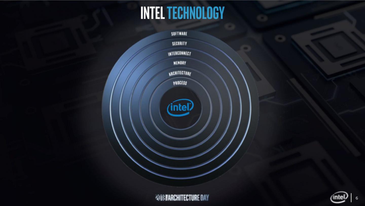
At Intel’s recent Architecture Day, Raja Koduri, Intel’s senior vice president of Core and Visual Computing, outlined a strategic shift for the company’s design and engineering model. This shift combines a series of foundational building blocks that leverage a portfolio of technologies and intellectual property (IP) within the company.
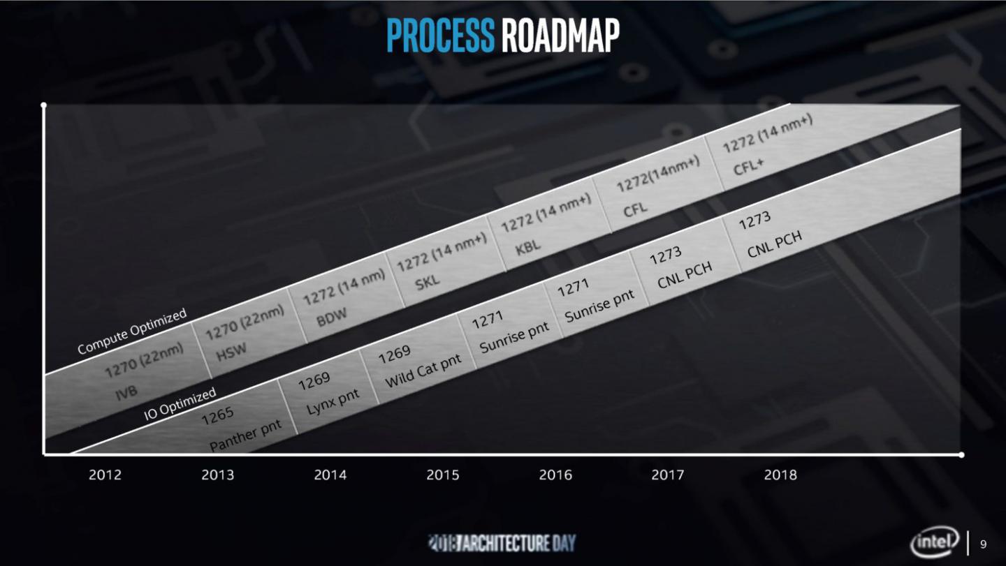
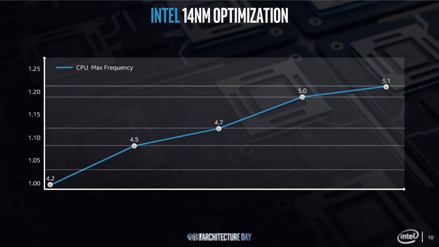
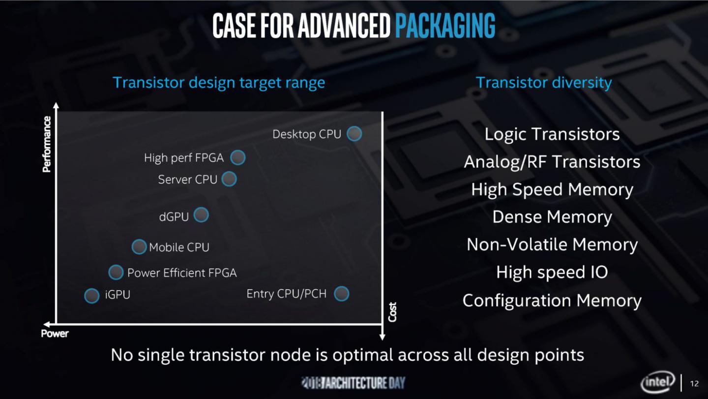
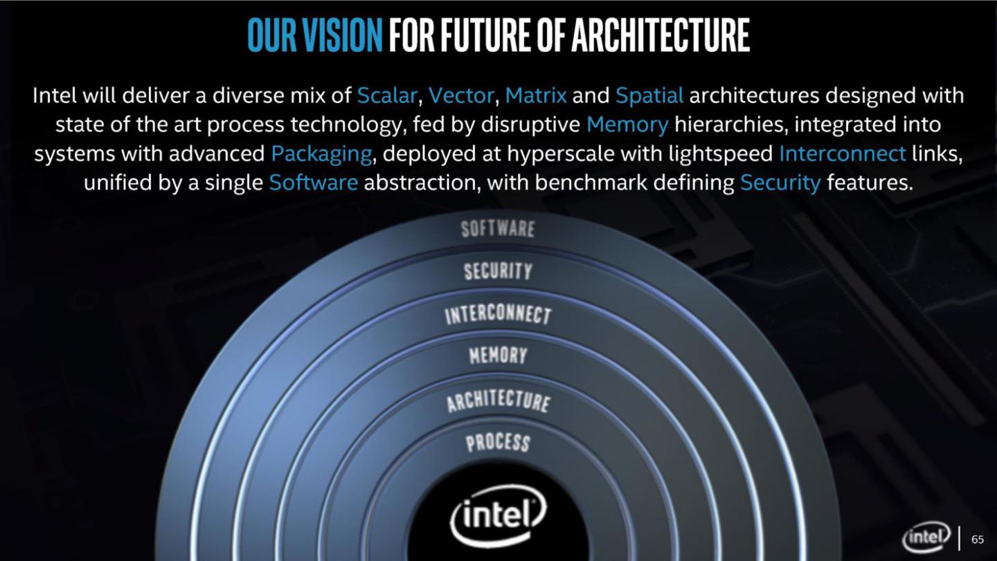
- Process: Access to leadership process technology remains essential to building leadership products. Advanced packaging solutions will enable Intel to continue exponential scaling in computing density by extending transistor density to the third dimension.
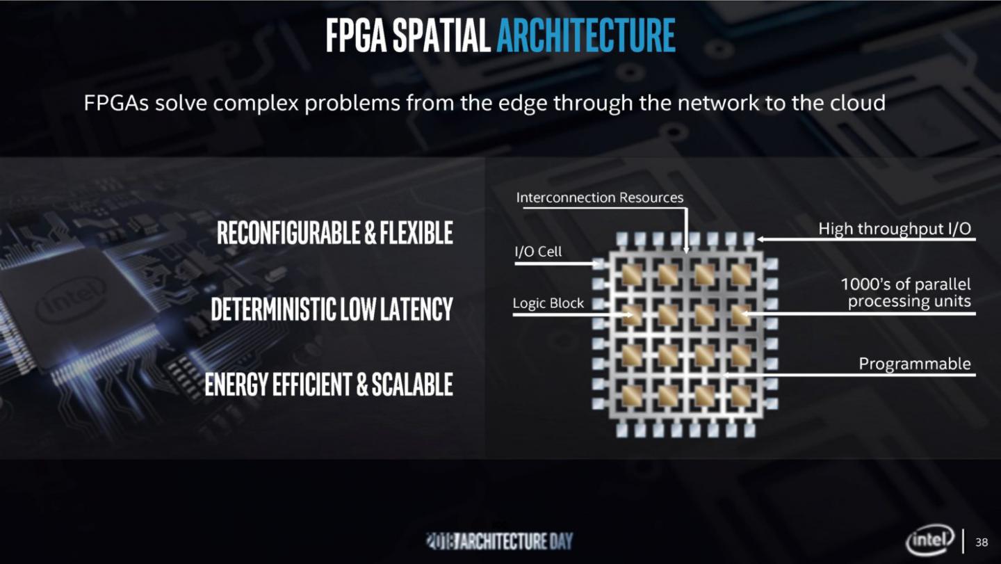
- Architecture: The future is a diverse mix of scalar, vector, matrix and spatial architectures deployed in CPU, GPU, accelerator and FPGA sockets, enabled by a scalable software stack, integrated into systems by advanced packaging technology.
- Memory: High-capacity, high-speed storage is crucial for next-generation computing workloads. Intel is uniquely positioned to combine in-package memory and Intel® Optane™ technology to fill gaps in the memory hierarchy to provide bandwidth closer to the silicon die.
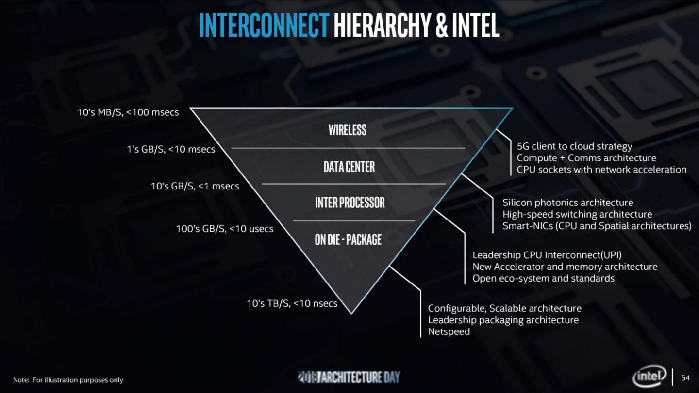
- Interconnect: Communication scales from wireless connections for 5G infrastructure to silicon-level package and die interconnects. Only by offering a complete range of leading interconnect products enables the heterogeneous computing landscape at scale.
- Security: With the emergence of new threats, Intel has all the components to build a “better together” security strategy. Intel is uniquely positioned to deliver security technologies that help improve the end-to-end and to make security advancements a key differentiator.
- Software: For every order of magnitude performance potential of a new hardware architecture there are two orders of magnitude performance enabled by software. A common set of tools that can address Intel silicon for developers is critical to exponential scaling.
Q&A – RAJA KODURI
Why do you believe that in this new era of computing Intel should anchor its product and technology strategy around these six pillars?
The landscape for computing has evolved dramatically over the past decade. We operate in a world where we generate data at a faster rate than our ability to analyze, understand and help secure it. We see immense demand for computing architectures that evolve rapidly and scale exponentially. We have a bold engineering vision over the next five years to deliver 10 petaflops of compute and 10 petabytes of data within 10 milliseconds to every person in the world. We believe these six technology pillars are the key enablers for us to drive the needed product innovation to achieve this.
How do the IP and resources in the six pillars best position Intel to win and deliver differentiated products from your competitors?
When I joined Intel, I was amazed at the sheer volume and breadth of IP available to us. In nearly three decades in the industry, I’ve never seen anything like it. The scale of these resources gives us a differentiated set of technologies in each of these pillars to apply as we drive wave after wave of innovation for client, edge and cloud computing environments. I believe we are uniquely positioned to deliver leadership across all six of these pillars which provides a foundation for sustained innovation nobody else can offer.
Why did the innovation model have to change?
The world has changed and so has our business; we’ve moved to target an addressable market north of $300 billion1. The rising demand for computing provides us with a chance to change, mold and expand Intel in an unprecedented manner. We have a responsibility not only to ourselves, but also to our customers who trust us with their businesses, critical data and computing needs, to reinvent our products and strategy for developing technologies for the next decade and beyond.
How is Intel applying the model today and in the future?
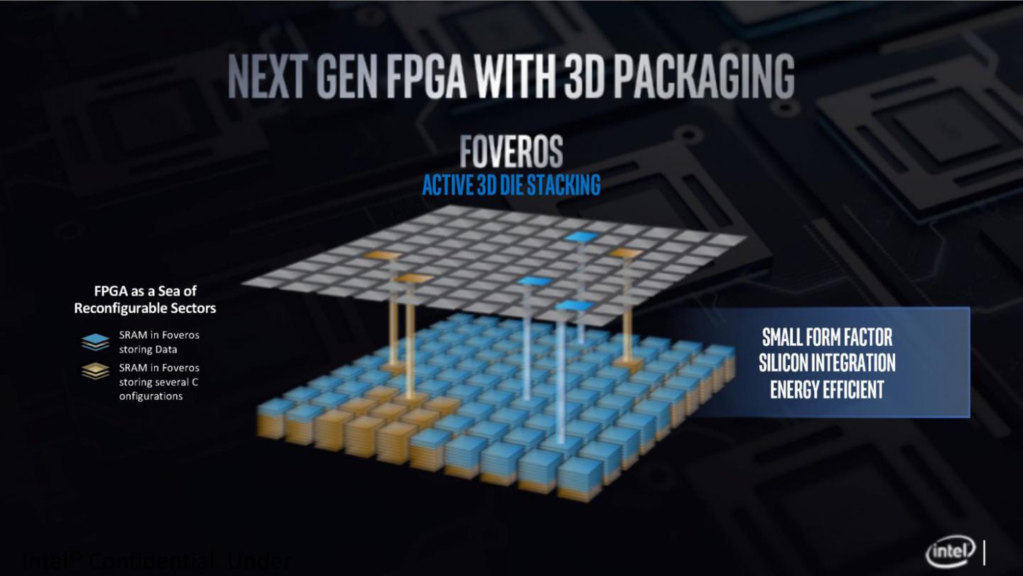
We’re applying the model today across our engineering organization as we bring innovative new product and technology initiatives to the world next year and into the future. Whether it’s the advanced packaging innovation through “Foveros” logic stacking or the “One API” approach to software developers, we’re taking steps to drive sustainable new waves of innovation.
How does the shifting landscape in computing workloads impact how Intel will build its next-generation products?
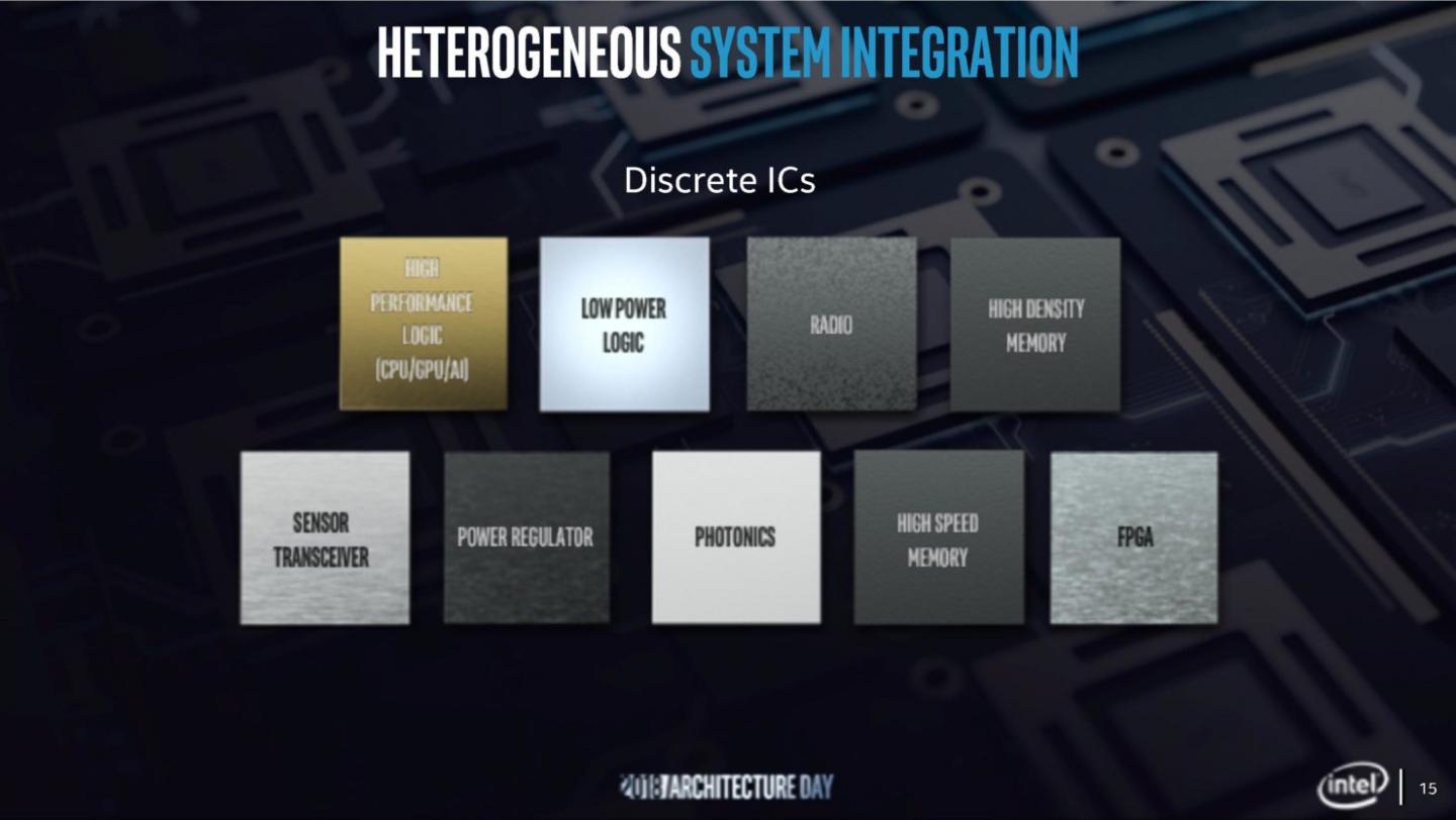
The workloads associated with this computing landscape are changing. No longer do consumers or enterprise customers have simple applications that can be addressed with straightforward scalar architectures alone. Instead we see programs that are solving problems faster by integrating additional architectures from graphics processors to artificial intelligence accelerators to image processors and even adaptable designs like FPGAs powered by new memory technologies. We will combine computing and architecture innovations through high-speed interconnects with new models for software development that simplify APIs for developers and allow more performance and efficiency to be unlocked from Intel computing architectures.
How do Intel’s investments in the six pillars drive Moore’s Law-like leaps forward in user experience?
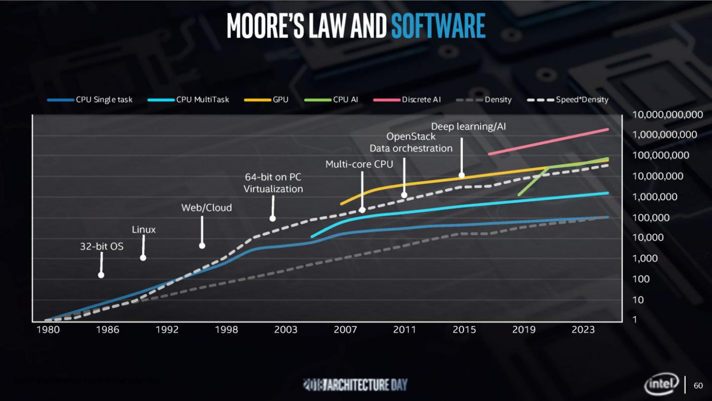
In the previous generations, the answer has been that transistor density and Moore’s Law will play the lead role to solve computing problems. But as the process node transitions have slowed from the pace of the previous decades, it is the essence of Moore’s Law that continues to provide new technologies and capabilities to meet the demands of modern computing. The message of Moore’s Law is about more than transistors alone, with the combination of transistors, architectural research, connectivity advancements, faster memory systems, and software working together to drive it forward.
Intel Architecture Day Highlights:
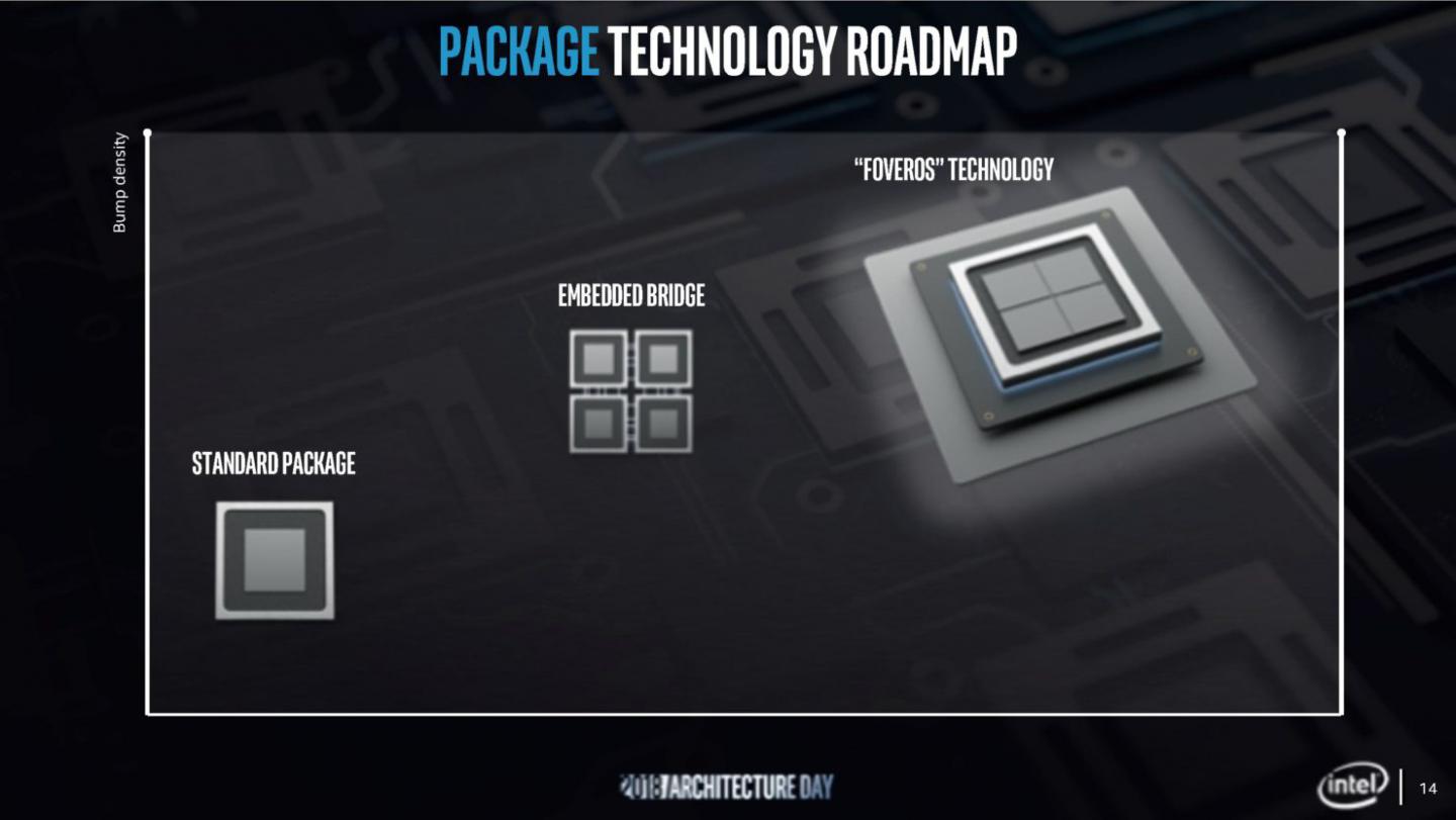
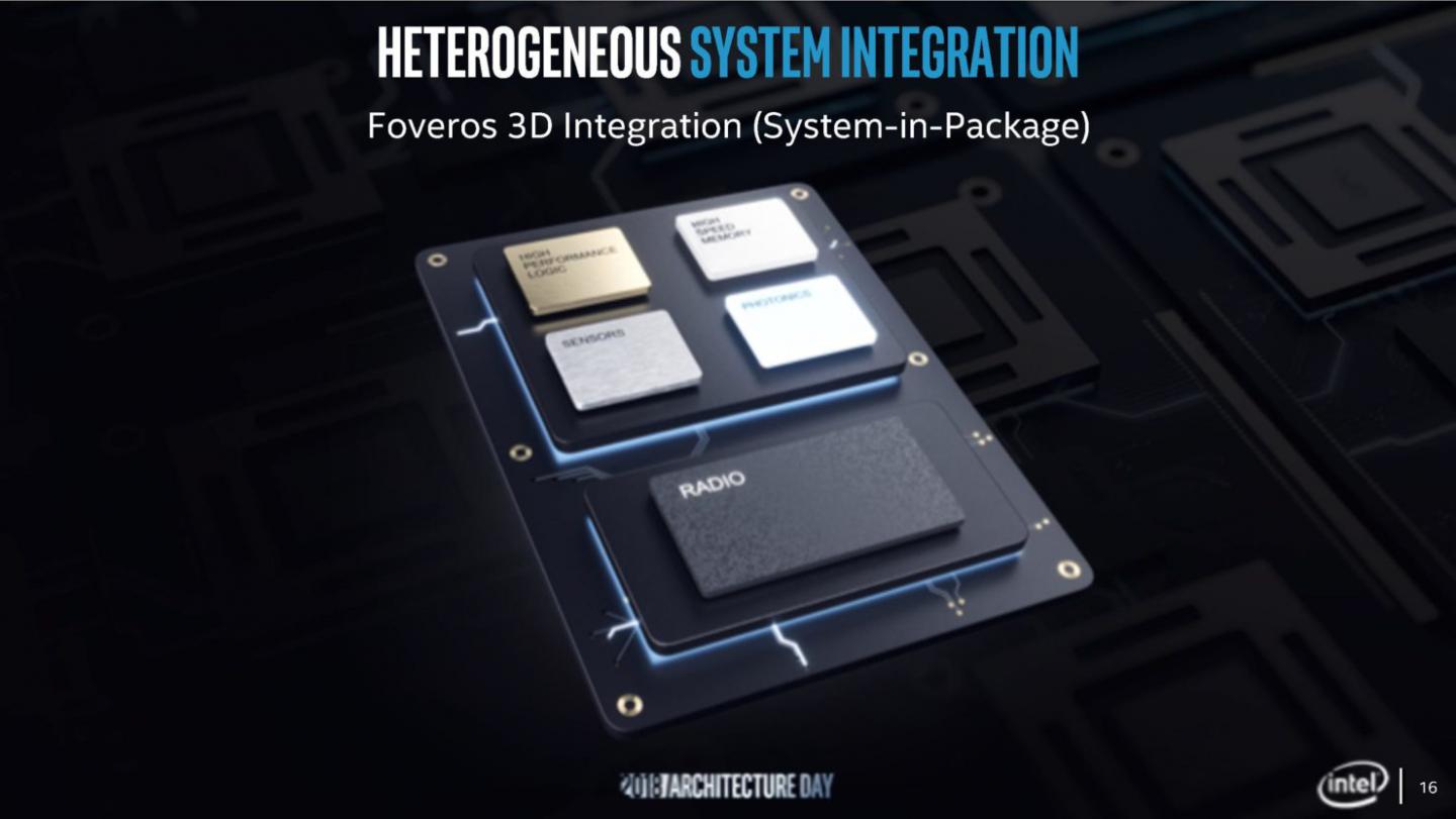
- Industry-First 3D Stacking of Logic Chips: Intel demonstrated a new 3D packaging technology, called “Foveros,” which for the first time brings the benefits of 3D stacking to enable logic-on-logic integration.
Foveros paves the way for devices and systems combining high-performance, high-density and low-power silicon process technologies. Foveros is expected to extend die stacking beyond traditional passive interposers and stacked memory to high-performance logic, such as CPU, graphics and AI processors for the first time.
The technology provides tremendous flexibility as designers seek to “mix and match” technology IP blocks with various memory and I/O elements in new device form factors. It will allow products to be broken up into smaller “chiplets,” where I/O, SRAM and power delivery circuits can be fabricated in a base die and high-performance logic chiplets are stacked on top.
Intel expects to launch a range of products using Foveros beginning in the second half of 2019. The first Foveros product will combine a high-performance 10nm compute-stacked chiplet with a low-power 22FFL base die. It will enable the combination of world-class performance and power efficiency in a small form factor.
Foveros is the next leap forward following Intel’s breakthrough Embedded Multi-die Interconnect Bridge (EMIB) 2D packaging technology, introduced in 2018.
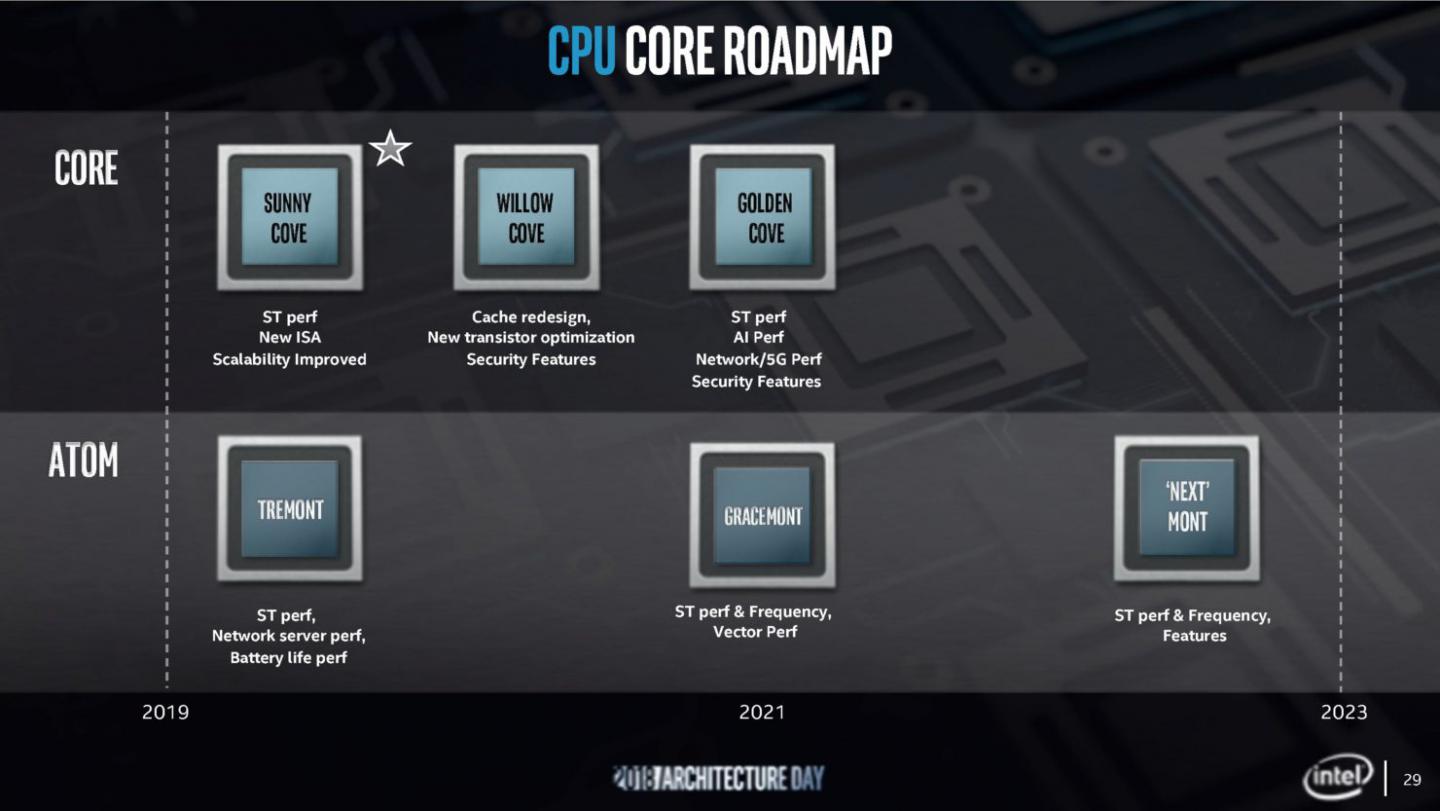
- New Sunny Cove CPU Architecture: Intel introduced Sunny Cove, Intel’s next-generation CPU microarchitecture designed to increase performance per clock and power efficiency for general purpose computing tasks, and includes new features to accelerate special purpose computing tasks like AI and cryptography. Sunny Cove will be the basis for Intel’s next-generation server (Intel® Xeon®) and client (Intel® Core™) processors later next year. Sunny Cove features include:
- Enhanced microarchitecture to execute more operations in parallel.
- New algorithms to reduce latency.
- Increased size of key buffers and caches to optimize data-centric workloads.
- Architectural extensions for specific use cases and algorithms. For example, new performance-boosting instructions for cryptography, such as vector AES and SHA-NI, and other critical use cases like compression and decompression.
Sunny Cove enables reduced latency and high throughput, as well as offers much greater parallelism that is expected to improve experiences from gaming to media to data-centric applications.
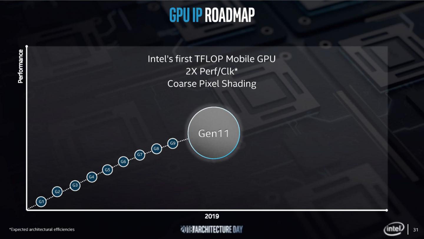
- Next-Generation Graphics: Intel unveiled new Gen11 integrated graphics with 64 enhanced execution units, more than double previous Intel Gen9 graphics (24 EUs), designed to break the 1 TFLOPS barrier. The new integrated graphics will be delivered in 10nm-based processors beginning in 2019.
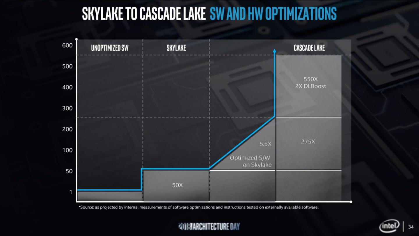
The new integrated graphics architecture is expected to double the computing performance-per-clock compared to Intel Gen9 graphics. With >1 TFLOPS performance capability, this architecture is designed to increase game playability. At the event, Intel showed Gen11 graphics nearly doubling the performance of a popular photo recognition application when compared to Intel’s Gen9 graphics. Gen11 graphics is expected to also feature an advanced media encoder and decoder, supporting 4K video streams and 8K content creation in constrained power envelopes. Gen11 will also feature Intel® Adaptive Sync technology enabling smooth frame rates for gaming.
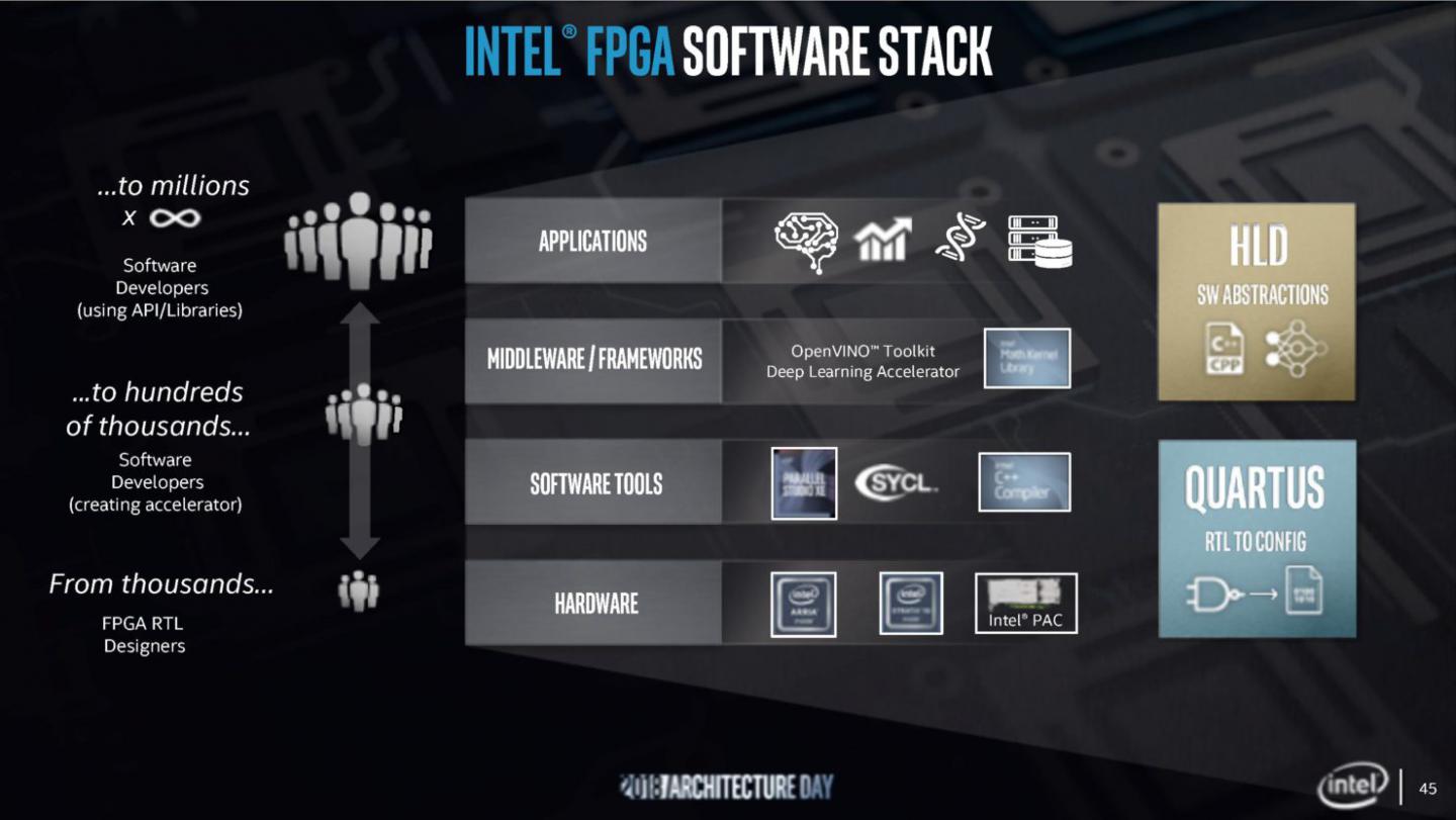
Intel also reaffirmed its plan to introduce a discrete graphics processor by 2020. - “One API” Software: Intel announced the “One API” project to simplify the programming of diverse computing engines across CPU, GPU, FPGA, AI and other accelerators. The project includes a comprehensive and unified portfolio of developer tools for mapping software to the hardware that can best accelerate the code. A public project release is expected to be available in 2019.
- Memory and Storage: Intel discussed updates on Intel® Optane™ technology and the products based upon that technology. Intel® Optane™ DC persistent memory is a new product that converges memory-like performance with the data persistence and large capacity of storage. The revolutionary technology brings more data closer to the CPU for faster processing of bigger data sets like those used in AI and large databases. Its large capacity and data persistence reduces the need to make time-consuming trips to storage, which can improve workload performance. Intel Optane DC persistent memory delivers cache line (64B) reads to the CPU. On average, the average idle read latency with Optane persistent memory is expected to be about 350 nanoseconds when applications direct the read operation to Optane persistent memory, or when the requested data is not cached in DRAM. For scale, an Optane DC SSD has an average idle read latency of about 10,000 nanoseconds (10 microseconds), a remarkable improvement.2 In cases where requested data is in DRAM, either cached by the CPU’s memory controller or directed by the application, memory sub-system responsiveness is expected to be identical to DRAM (<100 nanoseconds).
The combination of Intel Optane SSDs with QLC NAND SSDs will enable lower latency access to data used most frequently. Taken together, these platform and memory advances complete the memory and storage hierarchy providing the right set of choices for systems and applications.
- Deep Learning Reference Stack: Intel is releasing the Deep Learning Reference Stack, an integrated, highly-performant open source stack optimized for Intel® Xeon® Scalable platforms. This open source community release is part of our effort to ensure AI developers have easy access to all of the features and functionality of the Intel platforms. The Deep Learning Reference Stack is highly-tuned and built for cloud native environments. With this release, Intel is enabling developers to quickly prototype by reducing the complexity associated with integrating multiple software components, while still giving users the flexibility to customize their solutions.
-
- Operating System: Clear Linux* OS is customizable to individual development needs, tuned for Intel platforms and specific use cases like deep learning;
- Orchestration: Kubernetes* manages and orchestrates containerized applications for multi-node clusters with Intel platform awareness;
- Containers: Docker* containers and Kata* containers utilize Intel® Virtualization Technology to help secure container;
- Libraries: Intel® Math Kernel Library for Deep Neural Networks (MKL DNN) is Intel’s highly optimized math library for mathematical function performance;
- Runtimes: Python* providing application and service execution runtime support is highly tuned and optimized for Intel architecture;
- Frameworks: TensorFlow* is a leading deep learning and machine learning framework;
- Deployment: KubeFlow* is an open-source industry-driven deployment tool that provides a fast experience on Intel architecture, ease of installation and simple use.
Below some of the Architecture Day 2018 press deck: