Intel LGA 7529 Processors are Nearly 10cm in Length
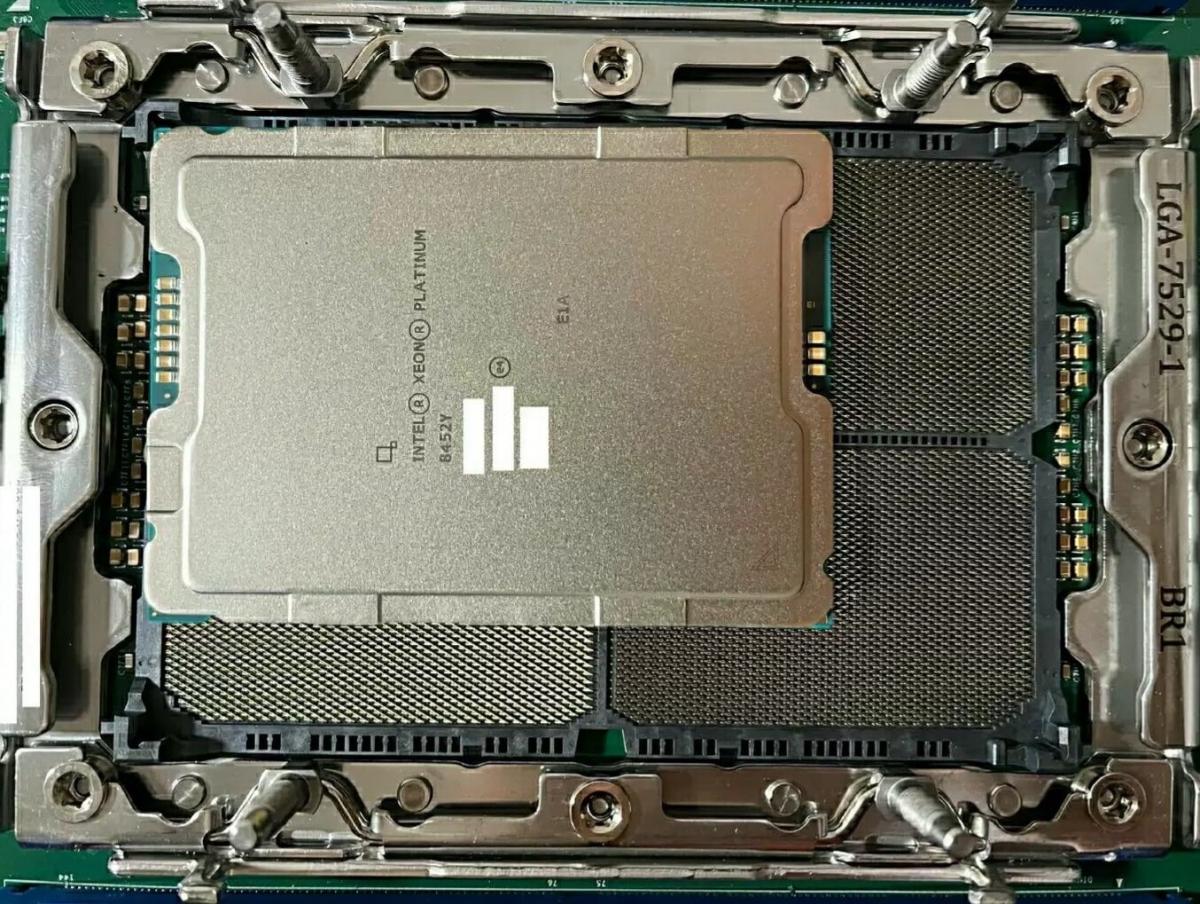
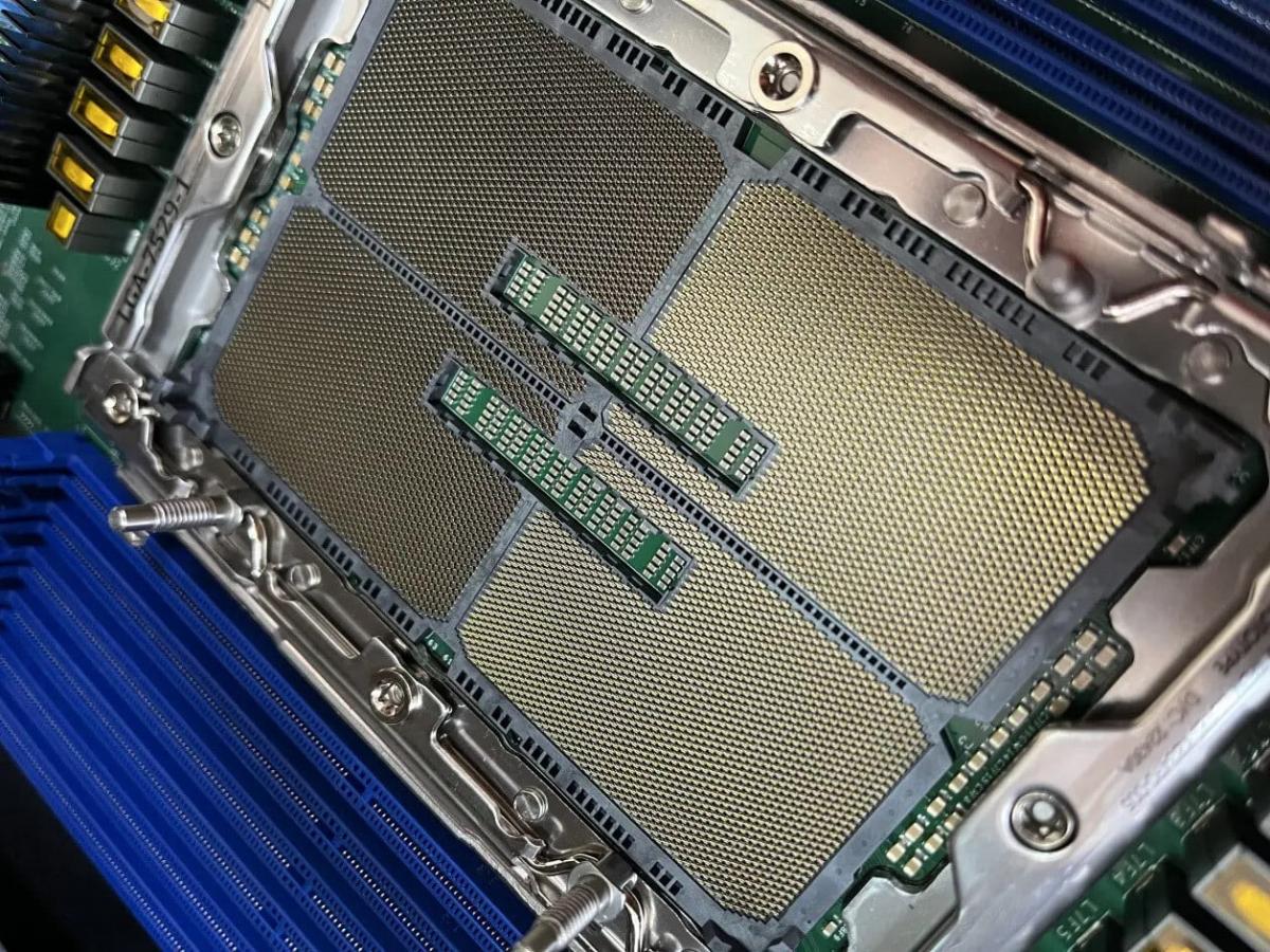
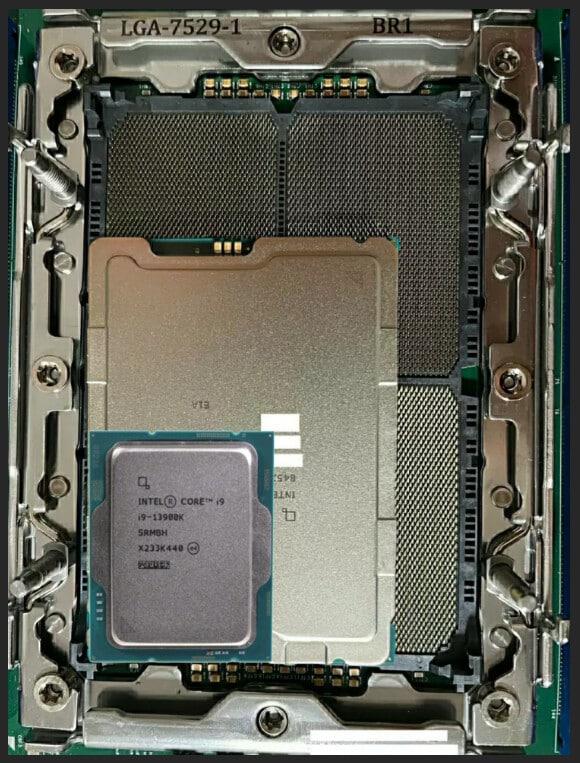
Recently, Bilibili, a Chinese website, published images of the LGA 7529 socket, confirming that the upcoming processors will be significantly larger than their predecessors.
Although the LGA 4677 was already considered large with dimensions of 61 x 82mm, the new "Mountain Stream" platform will surprise users with its size of 66 x 92.5mm, nearly 10 cm in length. The new platform is designed to work alongside Intel's Sierra Forest and Granite Rapids lines of CPUs and is scheduled for release in 2024.
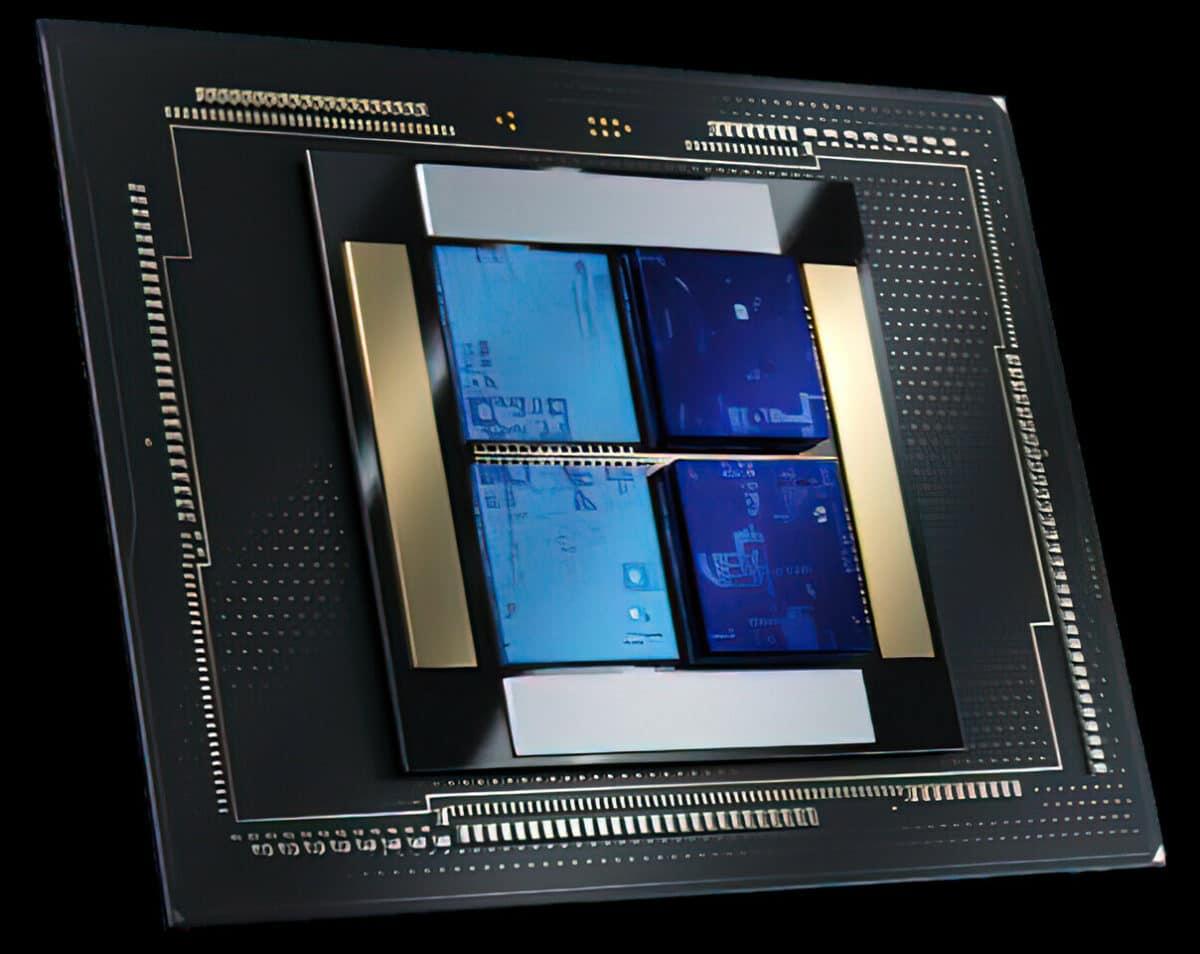
Industry analysts predict that Intel's fifth-generation Xeon microarchitectures, codenamed Avenue City, will revolutionize server and cloud computing. These processors will support dual-socket configurations and offer two distinct models. The P-Core variants will feature 86 and 132 cores, while the E-Core variants will range from 334 to 512 cores and include HBM variants. Recently leaked photos of the prototypes reveal the "ES" (engineer sample) inscription, indicating that they were designed for testing purposes.
Intel's commitment to delivering high-performance processors has driven the decision to abandon the LGA 1700 socket in favor of inline production, with Arrow Lake-S set to launch in 2023. As the launch date for the fifth-generation Xeon processors approaches in 2024, Intel is expected to provide more details about the new processors.
EK-Quantum Velocity expands to Intel LGA 1200 socket - 01/12/2022 09:48 AM
The water block showcases the EK-Matrix7 initiative, a standard where increments of 7mm manage the height of products and the distance between ports. This product uses a socket-specific cooling engine...
List of water blocks made by CORSAIR that are compatible with Intel LGA1700 processor: XC5 / XC7 RGB PRO - 12/10/2021 09:57 AM
There are new water blocks from CORSAIR's "Hydro X Series" that can be used with CPUs and have 16 RGB LEDs. The water blocks from CORSAIR's XC5 / XC7 RGB PRO series are compatible with...
Scythe announces the availability of a mounting upgrade kit for the Intel LGA1700 socket - 11/04/2021 09:43 AM
It is possible to use Scythe's mounting upgrade kit (SCMK-1700) in conjunction with Intel's forthcoming LGA1700 platform. The mounting upgrade kit enables Scythe users to adapt their coolers to Inte...
DeepCool includes free Intel LGA1700 CPU cooler installation kit - 10/22/2021 03:28 PM
Intel's 12th generation desktop processors will be unveiled in the near future. Because Alder Lake-S makes use of the larger lga1700 socket, it is necessary to purchase additional mounting hardware i...
be quiet! provides complimentary CPU cooler mounting kit for the Intel LGA 1700 socket - 09/29/2021 01:26 PM
be quiet!, the German manufacturer for premium PC components, ensures that its CPU coolers remain compatible with the latest CPU sockets. Therefore, the company will be offering a free upgrade kit for...
Senior Member
Posts: 3404
Joined: 2013-03-10
Considering the large CPUs are MCM based, the chips themselves already are sitting on a substrate. It seems to me the substrate wouldn't be that much thicker to handle the power distribution from far fewer outside points. At the end of the day, though, that would only make the outside of the CPU and the socket on the mobo more safe from external damage, as with the current tech, internally the CPU chiplets would still need that many points of power delivery via the substrate. Still, it would be nicer for anyone assembling a system.
Senior Member
Posts: 2479
Joined: 2016-01-29
I feel like there must be an upper limit to how many pins are actually needed. You need a finite amount to handle the PCIe lanes and memory channels; there's not really a point in having more than 128 PCIe lanes (unless you're doing something like AMD where you're linking the CPUs via PCIe) and there gets to be a point where you just simply can't fit all the traces on a motherboard for more memory channels. With how large these packages are, it makes sense to integrate more onto the SoC, thereby reducing the need of more pins leading elsewhere to the motherboard.
So unless I'm missing something here, that just leaves pins for power delivery. If 7529 becomes that huge just so all the cores can be fed more power, that's a rather bleak future. Perhaps Intel is intending to compete with AMD by having one gargantuan socket rather than multi-socket designs, which overall makes sense.
there are chips that are almost an entire wafer in size, and 128lanes of pcie is really no where near the maximum useful amount, bigger cpus mean more cores per rack , more cores per data center, bigger packages are the logical thing to do when die shrinks do not offer cost reductions and density increases you need to meet demands. you can do more pcb layers, so really there isnt any limit for that so far as you have the cash to pay for it. it is completely possible to have packages tbe size of a dinner plate or larger, it just a matter of cost and application.
Senior Member
Posts: 7424
Joined: 2012-11-10
Do you have an example of one of such chips? I can't imagine how that's done beyond some very niche applications, and likely using some rather large node.
Intel I think still uses UPI links to do inter-socket communication rather than PCIe, which means they have a much lower dependency on PCIe lanes than AMD. Regardless, most server motherboards from what I've seen barely have enough room for 64 lanes of PCIe expansion cards. Granted, a lot of such boards use a lot of their available lanes for things like integrated networking, but my point is: I haven't got the impression there's a demand for more lanes, but rather, faster lanes. So, I still don't see having more than 128 lanes being necessary any time soon, if ever.
There's really only 2 outcomes when it comes to scaling up a processor to such extreme levels:
A. The SoC is so powerful/capable that it reduces how much bandwidth it needs.
B. The demand is so immense that it completely dwarfs the SoC's potential, where it's probably be more cost effective to buy more servers of less potential.
It seems to me there's an upper limit to how much you can cram on a motherboard until it doesn't make economic sense. Since chiplets are basically just more tightly integrated multi-socket designs, I don't really see the purpose in having one gargantuan socket the size of an ITX motherboard with a PCB so thick you would need different chassis standoffs to mount it. By having multiple sockets, you reduce the cost of the package and you can cram more features on the motherboard since you don't have thousands of traces going to one spot.
Senior Member
Posts: 2479
Joined: 2016-01-29
Do you have an example of one of such chips? I can't imagine how that's done beyond some very niche applications, and likely using some rather large node.
Intel I think still uses UPI links to do inter-socket communication rather than PCIe, which means they have a much lower dependency on PCIe lanes than AMD. Regardless, most server motherboards from what I've seen barely have enough room for 64 lanes of PCIe expansion cards. Granted, a lot of such boards use a lot of their available lanes for things like integrated networking, but my point is: I haven't got the impression there's a demand for more lanes, but rather, faster lanes. So, I still don't see having more than 128 lanes being necessary any time soon, if ever.
There's really only 2 outcomes when it comes to scaling up a processor to such extreme levels:
A. The SoC is so powerful/capable that it reduces how much bandwidth it needs.
B. The demand is so immense that it completely dwarfs the SoC's potential, where it's probably be more cost effective to buy more servers of less potential.
It seems to me there's an upper limit to how much you can cram on a motherboard until it doesn't make economic sense. Since chiplets are basically just more tightly integrated multi-socket designs, I don't really see the purpose in having one gargantuan socket the size of an ITX motherboard with a PCB so thick you would need different chassis standoffs to mount it. By having multiple sockets, you reduce the cost of the package and you can cram more features on the motherboard since you don't have thousands of traces going to one spot.
here is the chip https://www.cerebras.net/blog/wafer-scale-processors-the-time-has-come/,(((wafer-scale)))
there is always room for more i/o, and more cores = more i/o. if amd could double the core count per package , they could double the io easily, you don't see much more than 16 layer pcbs on consumer hardware, but you can go beyond 24 layers, There is a long way to go before such things become impractical. If you're building a supremely large cluster or run a data center, more per rack means more throughput, at the current time there is practically infinite demand for computing resources, $30K racks aren't rare when a single xeon can set you back $10-20k, even something like a 24+ layer pcb is going to be a minor cost compared to the rest of the components, if you just think about a single compute node , which may comprise of 2 genoa cpus, and 12 gpus, the total silicon on that is huge, if you can wrap as much as you can into fewer larger packages, that saves you space, circuitry, and cooling complexity. its the obvious solution. and You should see some of the truly enormous mainframes from the past.
check this package out ,
computers were really big before stuff got small. and now due to technical limitations of shrinks, we're going big again. we've been kind of spoiled by node shrinks delivering performance uplift.
Industrial/commercial/government applications have very different requirements compared comsumer. and those giant xeons aren't for consumers, market conditions can support(and have supported) much larger packages.
Senior Member
Posts: 7424
Joined: 2012-11-10
I feel like there must be an upper limit to how many pins are actually needed. You need a finite amount to handle the PCIe lanes and memory channels; there's not really a point in having more than 128 PCIe lanes (unless you're doing something like AMD where you're linking the CPUs via PCIe) and there gets to be a point where you just simply can't fit all the traces on a motherboard for more memory channels. With how large these packages are, it makes sense to integrate more onto the SoC, thereby reducing the need of more pins leading elsewhere to the motherboard.
So unless I'm missing something here, that just leaves pins for power delivery. If 7529 becomes that huge just so all the cores can be fed more power, that's a rather bleak future. Perhaps Intel is intending to compete with AMD by having one gargantuan socket rather than multi-socket designs, which overall makes sense.