AMD seems to be making some changes for Sea Islands in order to respond to Nvidia's Kepler revision series of products. The new GPU family is now codenamed "Volcanic Islands" and is slated for late 2013, expect the Christmas season. The new Volcanic Islands GPU’s could be be manufactured on a 20nm Gate-Last process through either TSMC or Common Platform Alliance, but that remains unconfirmed though. We have some very intersting specs to share though.
According to reports coming from Chiphell Volcanic Islands could be coming in the last quarter and feature the Hawaii graphics core that is going to replace Tahiti (Tahiti is used in the series Radeon HD 7900 graphics cards). Now the Volcanic Islands architecture although not confirmed could very well stick to 28nm, but 20nm is more plausible if the chip foundries are ready for it. Two additional and possible codenames have been hinted as Reychavik and Honolulu, of which both are active volcanoes and or related to vulcanic islands.
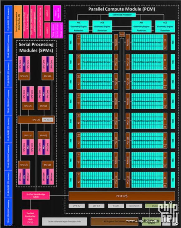
The chip codenamed Hawaii looks to be the most high-end part and would pack some serious muscle:
- 20 nm fabrication proces
- 4096 shader processors
- 16 serial processor units
- 4 geometry engines
- 256 TMUs
- 64 ROPs
- 512-bit GDDR5 memory interface
The early block Diagram has leaked through an Asian website Chiphell, showing "Hawaii," 20nm 16X SPU 4X ACE/Geometry Engine 4096SP 256TMU 64ROPs 512Bit.
The diagram is very blurry but you can see that there will be parallel and serial shader units embedded. If that is the case then AMD is making really significant changes in their architecture as the serial cores that AMD may use (licensing wise) are x86 and could help out on the compute side of things.
Now if we chart it up you can see why this is such big news, as this is a 2x performance increase over the current high-end graphics part.
| AMD Radeon HD 9970 Hawaii GPU | AMD Radeon HD 7970 Tahiti GPU | |
|---|---|---|
| Die Size | 20nm/28nm | 28nm |
| Stream Processors | 4096 | 2048 |
| Compute Units | 16 | 32 |
| TMUS | 256 | 128 |
| ROPS | 64 | 32 |
| Memory | 4 GB GDDR5 | 3 GB GDDR5 |
| Memory Bus | 512-bit | 384-bit |
As always, leaked information and slides like the block diagram shown above should be taken with a grain of salt. You never know if they are correct and the reality is that the block diagram does have the AMD 'feel and aesthetics their typical presentations have. But the leak of this block diagram is seriously significant, if right.