Intel Details Newest Microarchitecture and 14 NM Fab Process
Intel today disclosed details of its newest microarchitecture that is optimized with Intel's industry-leading 14 nm manufacturing process. Together these technologies will provide high-performance and low-power capabilities to serve a broad array of computing needs and products from the infrastructure of cloud computing and the Internet of Things to personal and mobile computing.
"Intel's integrated model - the combination of our design expertise with the best manufacturing process - makes it possible to deliver better performance and lower power to our customers and to consumers," said Rani Borkar, Intel vice president and general manager of product development. "This new microarchitecture is more than a remarkable technical achievement. It is a demonstration of the importance of our outside-in design philosophy that matches our design to customer requirements."
"Intel's 14 nanometer technology uses second-generation Tri-gate transistors to deliver industry-leading performance, power, density and cost per transistor," said Mark Bohr, Intel senior fellow, Technology and Manufacturing Group, and director, Process Architecture and Integration. "Intel's investments and commitment to Moore's law is at the heart of what our teams have been able to accomplish with this new process."
Key Points:
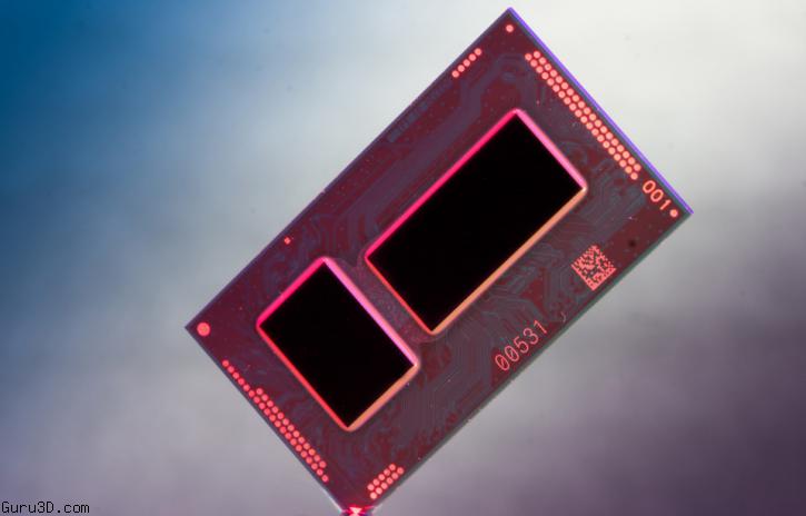
- Intel disclosed details of the microarchitecture of the Intel Core M processor, the first product to be manufactured using 14 nm.
- The combination of the new microarchitecture and manufacturing process will usher in a wave of innovation in new form factors, experiences and systems that are thinner and run silent and cool.
- Intel architects and chip designers have achieved greater than two times reduction in the thermal design point when compared to a previous generation of processor while providing similar performance and improved battery life.
- The new microarchitecture was optimized to take advantage of the new capabilities of the 14 nm manufacturing process.
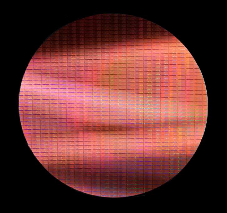
- Intel has delivered the world's first 14nm technology in volume production. It uses second-generation Tri-gate (FinFET) transistors with industry-leading performance, power, density and cost per transistor.
- Intel's 14 nm technology will be used to manufacture a wide range of high-performance to low-power products including servers, personal computing devices and Internet of Things.
- The first systems based on the Intel Core M processor will be on shelves for the holiday selling season followed by broader OEM availability in the first half of 2015.
- Additional products based on the Broadwell microarchitecture and 14 nm process technology will be introduced in the coming months.
Printed from: https://www.guru3d.com/story/intel-details-newest-microarchitecture-and-14-nm-fab-process/